Flatland exposed
Physicists are attracted to ideals. Real measurements, however, inevitably struggle with imperfect systems: an unwanted coupling to the environment or the presence of internal defects. Writing in Physical Review Letters, Kirill Bolotin and colleagues at Columbia University have produced graphene that is so clean they can explore the electron transport in a nearly ideal version of this atomically thin carbon sheet. By etching away the substrate and evaporating off adsorbants, they demonstrate that electrons in free-standing sheets of graphene can travel essentially without scattering over distances as long as —a sign that graphene is a realization of a nearly perfect two-dimensional electron system [1,2].
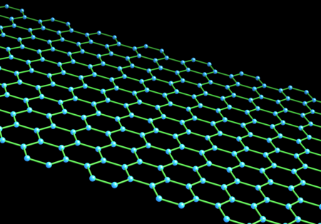
The two-dimensional nature of graphene originates from its atypical bonding. In most materials, chemical bonds accumulate electron density directly between two atoms. However, through an accident of the fundamental constants, the shapes of the atomic orbitals for boron, carbon, nitrogen, and oxygen allow these elements to form chemical bonds that accumulate charge perpendicular to the line connecting adjacent atoms. These -bonds (as opposed to -bonds which lie along the line between two atoms) are formed from the -orbitals and give these elements an exceptional diversity of closed-shell molecular bound states. In a solid, carbon’s ability to share charge “sideways” through -bonds enables it, unlike other elemental materials, to form an atomically thin two-dimensional sheet: graphene. Each atom makes three -bonds to its neighbors on a honeycomb lattice (see Fig. 1) and the entire sheet shares a collective -bond complex that spans the Fermi level.
Two-dimensional electron systems are a mature branch of semiconductor physics. Why then is graphene attracting such excitement? Up until now, two-dimensional electron systems were produced by layering dissimilar semiconductors to form a potential well for electrons within one of the layers. The confined electrons remember their parent material and so obey a quadratic energy-momentum relation similar to that of a bulk semiconductor, with distinct conduction and valence bands separated by a gap. The active layer is embedded deep below the surface.
In contrast, newborn graphene is naked and exposed to the elements. A fresh graphene surface rapidly adsorbs various molecules from the ambient air; these can modify the local electrostatic environment and might even hybridize directly with graphene states near the Fermi level. In addition, irregularities in the substrate underneath can deform a graphene sheet, scatter electrons, or induce a nonuniform distribution of charge [3–7]. Adsorbates can be removed by heating the material with a current that passes through electrical contacts. In their work, Bolotin et al. have developed a technique to eliminate the substrate as well. They etch away the silicon dioxide underneath a graphene flake to produce a clean suspended graphene membrane in a near-ideal geometry. With a gate electrode beneath the device, the group can precisely control the Fermi level in the graphene and measure its electron transport properties with unprecedented resolution.
What electronic properties are expected of ideal graphene? Materials whose Fermi energy falls within a gap in the density of states, , do not support low-energy electronic excitations; they are semiconductors or insulators. Graphene is unusual: the density of states does not have a gap at the Fermi level, as for a semiconductor, nor is it finite, as for a metal. Instead, decreases linearly to zero both above and below an energy called the charge neutrality point, which coincides with the Fermi level in ideal, pristine graphene. In addition, at low energy, the electron energy is linear in momentum rather than quadratic, as in a normal semiconductor. Electrons near the Fermi energy of pristine graphene can therefore be described as massless fermions, which leads to novel physics: Landau levels have an unusual structure, the quantum Hall effect has new plateaux and interfaces can generate lensing effects [8–14].
Imperfections disturb this scenario in two main ways, both of which the Columbia group have measured. Inhomogeneities over distances that are long compared to the wavelength of the charge carriers, such as slow variations in the surface density of adsorbates, shift the electron eigenstates up and down in an irregular energy landscape, In a normal metal, such inhomogeneities are inconsequential, since they are screened out within a few angstroms of a metal surface. But every atom of graphene is at the surface and the screening is weak because the density of states is low. Therefore, even small nonuniformities in the external potential can degrade the precision with which a gate electrode can specify the character of the highest-energy filled states. The most interesting such target is the charge neutrality point itself, where the density of states is exactly zero. The group measured the resistivity of a suspended graphene sheet as a function of the gate voltage, and managed to approach the ideal charge neutrality point more closely, perhaps, than ever before. The group estimates that the charge density at the neutrality point in their suspended graphene samples fluctuates by only electron per square micron, an extraordinarily low value, particularly as the sample itself is only microns across.
Shorter-range imperfections in the substrate, adsorbates, or graphene itself, such as individual lattice defects, scatter current-carrying electron waves, degrading the electrical conductivity and obscuring the contribution from intrinsic lattice vibrations (phonons). For normal metals, conductivity decreases with increasing temperature, since scattering between electrons and phonons increases as the lattice becomes more highly excited. In contrast, charge carriers in an insulator are thermally excited, so an insulator’s conductivity generally increases with increasing temperature. Clean suspended graphene shows both behaviors. If the gate biases the graphene close to the neutrality point, the conductivity increases with increasing temperature, as if an insulator, but it remains extremely high, as if a metal. When Bolotin et al. pull the Fermi energy farther from the neutrality point, the conductivity decreases with increasing temperature, as in a metal. Moreover, the group has determined that the charge carrier mobility, measured as an electron drift velocity per unit electric field (cm/s per V/cm), is the highest yet seen in any material: . Certain imperfections, namely the edges of the sample, are inescapable: conduction in a sufficiently clean and cold metal is dominated by edge effects. This regime is called “ballistic conduction,” since a wave packet in the interior of such a sample can propagate long distances without disturbance. In suspended graphene, near-ballistic transport over microns—which in most materials occurs at cryogenic temperatures—is sustained up to strikingly high temperatures.
Many practical applications, ironically, function because of their imperfections such as tangled dislocation lines that can strengthen a work-hardened metal or surface imperfections can act as catalysts. Suspended graphene may afford similar opportunities: with its sensitivity to environmental contaminants it could function as a sensor. Sometimes, new fundamental physics is enabled by controlled imperfections. For example, a bent graphene membrane could support extremely inhomogeneous fields: electrons respond primarily to the in-plane electric field and the out-of-plane magnetic field. If a sheet is bent sharply, then the perpendicular (parallel) component of an external magnetic (electric) field undergoes an extremely rapid shear.
On a more esoteric note, suspension makes the top and bottom surfaces of graphene indistinguishable, and the symmetry that the Columbia group achieves provides a way to invert the handedness of a micron-scale object. Whereas a left-handed leather glove turned inside out can be distinguished from a right-handed glove because the smooth and rough sides of the leather are reversed, a buckled graphene sheet popped inside out would become a perfect chiral invert of the original structure. Such buckling could be created by in-plane compression or the presence of pentagons and/or heptagons within the otherwise hexagonal honeycomb network of graphene; this buckling breaks this mid-plane reflection symmetry globally while preserving it locally.
In the cinema, the willing suspension of disbelief opens up a world of fantastic possibility. In two-dimensional physics, the suspension of a graphene leaf may open up equally grand opportunities.
References
- K. I. Bolotin, K. J. Sikes, J. Hone, H. L. Stormer, and P. Kim, Phys. Rev. Lett. 101, 096802 (2008)
- X. Du, I. Skachko, A. Barker, and E. Y. Andrei, Nature Nanotech 3, 491 (2008)
- S. Adam, E. H. Hwang, V. M. Galitski, and S. Das Sarma, Proc. of the Natl Acad. of Sci. 104, 18392 (2007)
- J.-H. Chen, C. Jang, S. Xiao, M. Ishigami, and M. S. Fuhrer, Nature Nanotech. 3, 206 (2008)
- S. V. Morozov, K. S. Novoselov, M. I. Katsnelson, F. Schedin, D. C. Elias, J. A. Jaszczak, and A. K. Geim, Phys. Rev. Lett. 100, 016602 (2008)
- M. I. Katsnelson, and A. K. Geim, Philos. T. Roy. Soc. A 366, 195 (2008)
- S. Fratini and F. Guinea, Phys. Rev. B 77, 195415 (2008)
- K. S. Novoselov, A. K. Geim, S. V. Morozov, D. Jiang, M. I. Katsnelson, I. V. Grigorieva, S. V. Dubonos, and A. A. Firsov, Nature 438, 197 (2005)
- Y. Zhang, Y.-W. Tan, H. L. Stormer, and P. Kim, Nature 438, 201 (2005)
- F. D. M. Haldane, Phys. Rev. Lett. 61, 2015 (1988)
- V. P. Gusynin and S. G. Sharapov, Phys. Rev. Lett. 95, 146801 (2005)
- M. I. Katsnelson, K. S. Novoselov, and A. K. Geim, Nat Phys 2, 620 (2006)
- Y. Zhang, et al., Phys. Rev. Lett. 96, 136806 (2006)
- D. A. Abanin, et al., Phys. Rev. Lett. 98, 196806 (2007)


