Making the probe the center of the experiment
An advance that has greatly simplified atomic-resolution imaging with electron microscopy is the introduction of components that compensate for the geometric aberration intrinsic to round electron lenses [1,2]. Transmission electron microscopy (TEM) can now produce micrographs that do not suffer from unwanted image aberrations [3], while the aberration-corrected optics in scanning transmission electron microscopy (STEM) make it possible to focus an electron beam to a spot size significantly smaller than the distance between atoms in a solid [4]. Both techniques can yield artifact-free micrographs that unambiguously reflect the atomic structure of the material being imaged. Moreover, these ultrahigh resolution probes (they have roughly three to four times higher resolution than conventional electron microscopes) are excellent tools for understanding the configuration of local defects, the structure of interfaces, and even the atomic arrangement of tiny nanoparticles.
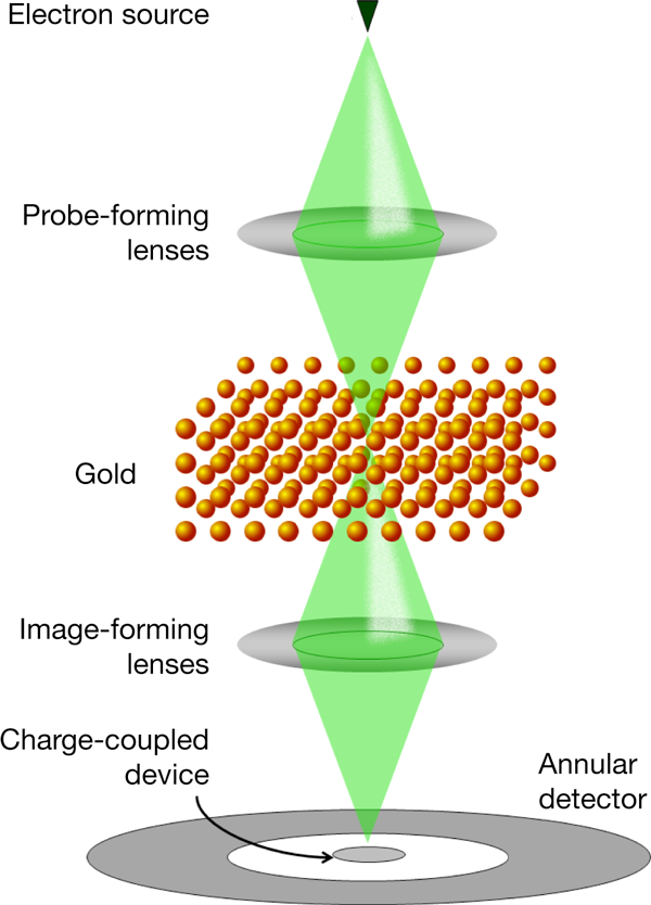
It is perhaps a subtle point, but micrographs are images of the materials under investigation, not the electron scattering itself. If the latter could be observed, however, it would provide direct insight into the electron-specimen interaction and thus reveal the physical mechanism that underlies the formation of images. In a paper appearing in Physical Review Letters, Joanne Etheridge, at Monash University in Australia, and co-workers [5] demonstrate that an electron microscope (Fig. 1) equipped with two aberration correctors—one forming the illumination spot and the other collecting the image—can be set up in such a way that one can directly observe how an electron probe, focused to an atomically sized spot, is site-specifically scattered by a crystalline object. Unlike TEM or STEM imaging, where the images are formed because the incoming electron beam is diffracted by the object, the experimental setup introduced by Etheridge and co-workers enables the observation of the electron beam as it is scattered by the crystal. This setup can record, in real space, the scattering of an electron probe as it site-specifically interacts with atoms in a crystal, a type of information that was previously only accessible by carrying out simulations, but which is essential for interpreting the information in micrographs.
Diffraction techniques are indispensible in applied physics, materials science, and biology. A diffraction pattern provides a direct map of the reciprocal space of a sample—a Fourier transform of the sample’s charge distribution. In principle, this map contains all of the information about the local atomic structure of a material, as well as information about distortions, local- and long-range order phenomena, and in some cases, the shape of the particles. Yet a diffraction pattern is indirect evidence that a crystal coherently scatters an incoming bundle of rays. However, what occurs locally inside the crystal is conjectured by the intensity distribution that is measured in the diffraction plane. In general, information about how the electron wave traveled through (and interacted with) the specimen is not accessible.
To access this information, Etheridge et al. devised a two-lens electron microscope. In principle, this setup is similar to a confocal STEM [6] except the electron beam has a narrower convergence angle. (Narrower convergence angles average over a larger thickness of the specimen, but in Etheridge et al.’s experiments, this was not an important limitation.) The first lens in their setup (Fig. 1) is in front of the specimen and forms a demagnified image of the pointlike electron source in the first lens’ focal plane. Behind the first lens, the second lens forms an enlarged image of the electron probe. However, what are simply referred to as lenses one and two are, in fact, an illumination system and an imaging system, each with an aberration corrector. The “lenses” are thus quite complex units that make it possible to form images in each step that are essentially free of aberrations. The output of this two-lens system is a magnified image of a demagnified electron source, which in itself may seem like a closed loop. Yet when a specimen of a few tens of nanometers in thickness is inserted in the focal plane of the first lens, the electron probe scatters inside the specimen. The image that results in the focal plane of the second lens is then the intensity distribution at the exit surface of the specimen imaged at the focal plane of the first lens. Recording this intensity distribution with a CCD camera, one obtains an image of the electron probe as it is scattered inside the crystal. Moreover, if the electron probe focused into the specimen is small enough (of the order of an angstrom) the electron probe can be positioned at different lateral positions, even within one projected unit cell of the crystal. Etheridge and co-workers [5] show that the intensity modulations the electron probe experiences due to scattering inside the crystal can be monitored with a precision of . This makes it possible to identify with which atoms within the specimen the electron probe interacts, as a function of the probe’s initial lateral position. Such a setup can, for example, be used to determine the local symmetry of a spot in a crystal.
But how can the electron probe be positioned on a specific site on the crystalline specimen? Etheridge and co-workers developed a new scanning transmission imaging technique to solve this problem [5]. Their real-space STEM or “R-STEM” imaging mode makes use of electrons that are deflected by higher-order aberrations of the imaging system. Though these residual higher-order aberrations are largely irrelevant for the smaller angle electrons that form the image of the electron probe, they have a more pronounced effect on electrons passing the imaging lens at high angles. Hence, as these electrons are displaced from the image of the electron probe, they can be collected with an annular detector in the exact same plane as the electron image itself. This is different from a standard STEM setup where the detectors are located in a diffraction plane in order to select electrons according to their specific scattering angle [7]. The R-STEM imaging technique makes it possible to record a STEM image immediately before positioning the probe on a specific site on the specimen and thus to control the experiment. No switching between modes is necessary.
Etheridge et al. used a - electron beam in a double aberration-corrected transmission electron microscope to study a gold foil oriented with its ( ) crystal axis along the beam path [5]. After recording a R-STEM image of the crystal, they positioned the electron probe on an atomic column and scanned the probe of diameter in ten steps along a direction in the gold foil to an equivalent column of gold atoms a distance of about away. At each of the ten positions, which are about apart, they recorded the electron probe as it is site-specifically scattered inside the crystal and observed how the scattering of the electron probe changes with the position of the probe. (For this reason, the experiment demands high beam stability and low sample drift and mechanical vibration.) The experimental results were then compared with simulations, which convincingly confirmed the experimental results.
One interesting experiment will be to try to observe if an electron probe channels along an atomic column, and, in particular, under which circumstances it de-channels to neighboring atomic columns. Channeling describes the trapping of an electron in the eigenstate of the electrostatic potential well formed by a column of atoms [8]. The technique may thus be helpful in understanding the image contrast in STEM images of more complex crystals consisting, for instance, of heavy cations and light anions, such as in cubic tungsten oxide ( ). A major question to be addressed is whether an electron probe positioned on a light anion site channels along the light oxygen column or de-channels to a neighboring heavy tungsten column, providing “fake” image scattering contrast at the oxygen sites. Though this seems to be an academic example, it comes back to the question of whether the information in TEM and STEM is specific to the atomic columns and whether the signal of individual atomic columns can reliably be used to perform chemical analysis with micrographs [9]. Indeed, such experiments can be expanded in order to deepen the understanding about the information contained in electron energy-loss spectra recorded at atomic resolution. So far, this issue, which is an ongoing controversial question, has mainly been addressed with theory. In this sense, Ehteridge et al.’s ability to monitor an electron probe as it scatters inside a crystal can be considered the ultimate electron probe experiment.
References
- M. Haider et al., Nature 392, 768 (1998)
- O. L. Krivanek, Inst. Phys. Conf. Ser.153, Sect. 2, 35 (1997)
- C. L. Jia, and K. Urban, Science 303, 2001 (2004)
- R. Erni et al., Phys. Rev. Lett. 102, 096101 (2009)
- J. Etheridge, S. Lazar, C. Dwyer, and G. A. Botton, Phys. Rev. Lett. 106, 160802 (2011)
- P. D. Nellist et al., Appl. Phys. Lett. 89, 124105 (2006)
- A. V. Crewe, Science 154, 729 (1966)
- A. Howie, Phil. Mag. 14, 223 (1966)
- S. Van Aert et al., Ultramicroscopy 109, 1236 (2009)