Spin Transport Goes Ballistic
The circuits in today’s computers, cell-phone cameras, and many other electronic devices rely on the manipulation of electronic charges via CMOS technology—transistors built from a combination of “complementary” metal, oxide, and semiconductor materials. A promising “beyond-CMOS” technology [1] is spintronics, in which information is carried by spin instead of charge. Spintronics devices could consume less power than CMOS devices and enable new applications. But efficiently injecting spins into conducting, two-dimensional channels, such as those that would be used in a spin-based version of the transistor, is difficult because of the large impedance mismatch between the spin “source” (typically a ferromagnet) and the channel, a result of the very different electronic density of states in the two materials. Now, researchers led by Dieter Weiss at the University of Regensburg, Germany, have achieved a high spin-injection efficiency from a ferromagnetic metallic semiconductor into the highly conducting two-dimensional electron gas that forms at the interface between two semiconductors [2]. In addition to expanding the types of materials that can be used in spintronics, their experiments reveal spin-transport effects that can’t be explained by existing models, and may open up new ways of thinking about spintronic devices.
In the early 1990s, a number of researchers set out to make the spin equivalent of the field-effect transistors (FETs) used in modern electronics. The idea behind this “spin FET,” a device proposed by Datta and Das [3], was that the spin state in the conducting channel and the corresponding analogic output signal could be modulated via a voltage gate. The key challenge for making such a device is to find a way to efficiently inject spins into the channel, which can be subsequently gated. (Efficiency is defined as the difference between a spin-up current and a spin-down current relative to the total current, and provides a “figure of merit” for charge to spin conversion.)
Two solid-state templates are considered the best candidates for making a spin FET and other spintronics devices. One is the high-mobility, semiconducting two-dimensional electron gas (2DEG) that can be formed at the interface of two semiconductors. This structure, which is what Weiss and his colleagues study, is typically made of III-V semiconductor compounds. The other option is graphene sheets—either a single layer or multiple layers—in which electrons have a high carrier mobility and high carrier velocity [4,5]. In semiconductor 2DEGs, the spin-orbit interaction is large, which allows the spin current to be manipulated by a voltage gate [6]. In graphene, electrons have longer spin diffusion times and spins can be injected (and converted back to electrical charges) with a high efficiency.
In a typical spintronics device, the 2D material used to transport the spins is formed into a (sub-) micron-sized channel. Two ferromagnetic metal contacts on the top of the channel function as a spin injector and spin detector that convert, respectively, an electric voltage into a spin current and vice versa. For most applications, the spin current has to be highly polarized and the spin population has to be unbalanced prior to any spin manipulation via a gate [6].
The device studied by Weiss and his colleagues consists of a high-mobility 2DEG formed at the interface between the semiconductors (Al,Ga)As and GaAs. In this 2DEG, the electrons are highly mobile and have a mean free path (mfp) of 4 micrometers ( m). (Ga,Mn)As serves as the ferromagnetic material for the source and drain contacts, which are and in size and therefore, respectively, smaller and similar to the mfp of electrons. The direct contact between (Ga,Mn)As and (Al,Ga)As forms a highly resistive (electrical) tunnel barrier, called an Ezaki diode. By injecting a small current (in the microampere range) from the contact, the authors generate a spin-polarized current that diffuses and travels a few micrometers along the 2DEG channel to the drain, where it outputs a “signal voltage” proportional to the spin current (and by extension, the spin injection efficiency) [7]. This detected voltage is on the order of microvolts and corresponds to a spin-resistance of the semiconducting channel on the order of ohms—a level expected from the standard theory of spin transport and thus clear evidence that a spin-polarized current has been generated and detected. For these small currents, the researchers’ measurements are consistent with a spin injection efficiency of .
Some of their findings, however, don’t fit with existing, state-of-the-art theory, and this is, perhaps, the most exciting aspect of the work. When they varied the bias voltage at the source to increase the injected spin current, the signal voltage rose by more than an order of magnitude. Using the standard theory to interpret their measurements would imply a spin injection efficiency of several hundred percent—clearly an unphysical number. The authors argue that this discrepancy occurs because standard theory assumes spins travel diffusively, while the spins in their device, which have a mfp comparable to the device dimensions, travel ballistically. Two of their experimental observations support this hypothesis. First, when they invert the source and drain and use the detector contact, which is larger than the mfp, to inject the spins, the signal enhancement goes away—a sign that the effect doesn’t have the reciprocity between spin-to-charge conversion expected from standard theory [8]. Similarly, when they study 2DEGs made from (In,Ga)As, in which electrons have a much shorter mfp than those made with GaAs, the enhanced signal voltage disappears. The present work thus demonstrates a new ballistic magnetoresistance effect that hasn’t been observed before.
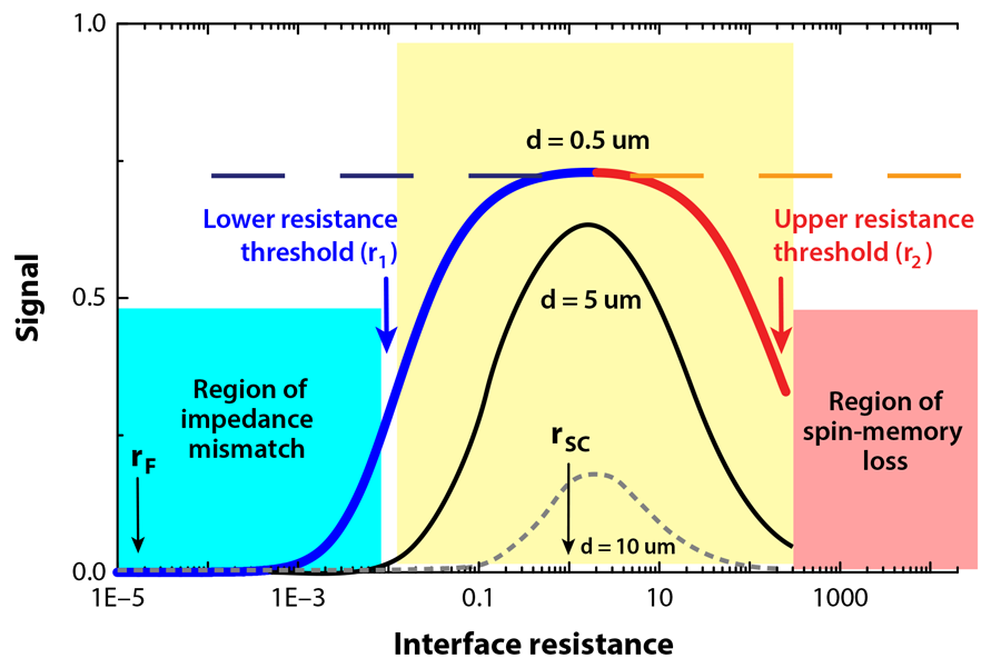
Signal enhancements because of ballistic effects can occur in spintronics devices, but the mechanism is different from what Weiss and his colleagues have found. As shown in Fig. 1, in most spintronic devices, the contact resistance between the ferromagnet and the semiconductor has to be carefully chosen to optimize the output signal [9]. The lower resistance threshold ( ) is necessary to overcome the “impedance mismatch” between the ferromagnetic metal and the semiconductor, which have very different density of states. The upper threshold ( ) is necessary, because if the barrier resistance is too high, the spin carriers will be reflected at the contacts and travel many times back and forth in the channel (Fig. 1), losing their spin information before reaching the detector. In such a setup, ballistic effects can explain a signal enhancement in the “low-resistance” window, below , in the regime where the impedance mismatch dominates the transport [9] (see Fig. 1). Here, having a ferromagnetic contact size that is smaller than the mfp largely helps to prevent the backward diffusion of spin to the injection contact (“back flow”) and keeps the spin-current high.
What is surprising about the work by Weiss and his colleagues is that the signal enhancement occurs well above the threshold, in the regime of high tunnel resistance. While it remains to be understood theoretically, this “ballistic” spin amplification could offer a promising way to optimize spin signals in future devices.
This research is published in Physical Review Letters.
References
- 2011 International Technology Roadmap for Semiconductors (International SEMATECH: Austin, TX, 2011); www.itrs.net/Links/2011ITRS/Home2011.htm
- M. Oltscher, M. Ciorga, M. Utz, D. Schuh, D. Bougeard, and D. Weiss, “Electrical Spin Injection into High Mobility 2D Systems,” Phys. Rev. Lett. 113, 236602 (2014)
- S. Datta and B. Das, “Electronic Analog of the Electro-Optic Modulator,” Appl. Phys. Lett. 56, 665 (1990)
- N. Tombros, C. Jozsa, M. Popinciuc, H. T. Jonkman, and B. J. van Wees, “Electronic Spin Transport and Spin Precession in Single Graphene Layers at Room Temperature,” Nature 448, 571 (2007)
- B. Dlubak et al., “Highly Efficient Spin Transport in Epitaxial Graphene on SiC,” Nature Phys. 8, 557 (2012); For a recent review see, e.g, P. Seneor, B. Dlubak, M.-B. Martin, A. Anane, H. Jaffrès, and A. Fert, “Spintronics with Graphene,” MRS Bulletin 37, 1245 (2012)
- H. C. Koo, J. H. Kwon, J. Eom, J. Chang, S. H. Han, and M. Johnson, “Control of Spin Precession in a Spin-Injected Field Effect Transistor,” Science 325, 1515 (2009)
- The measurements are performed at K so as to be below the Curie temperature of the (Ga,Mn)As
- H. Jaffrès, J. M. George, and A. Fert, “Spin Transport in Multiterminal Devices: Large Spin Signals in Devices with Confined Geometry,” Phys. Rev. B 82, 140408 (2010)
- A. Fert and H. Jaffrès, “Conditions for Efficient Spin Injection from a Ferromagnetic Metal into a Semiconductor,” Phys. Rev. B 64, 184420 (2001); For a review see A. Fert et al., “Semiconductors Between Spin-Polarized Sources and Drains,” IEEE Trans. Electron. Devices 54, 921 (2007)