Dowsing for Silicon
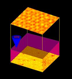
“Dowsers” claim to detect underground water without digging, using a magical forked tree branch. In the 1 June PRL, a team demonstrates the atomic-scale equivalent by imaging the nuances of a silicon surface buried deep under a layer of lead. Using a scanning tunneling microscope (STM), they obtained a surprisingly clear view of the buried interface, suggesting that the many physicists who make atomic-scale layered structures could benefit from the technique.
In a paper last year, Dongmin Chen, of the Rowland Institute for Science in Cambridge, MA, and his colleagues, demonstrated the “quantum wedge,” where they deposited lead atoms on top of a “staircase” of silicon “terraces.” Imaging the atomically smooth top surface of the lead, they saw alternating light and dark stripes that reflected the underlying silicon staircase, where each step changed the lead thickness by one atomic layer. The STM sees only electrons, but the stripes are analogous to the colorful interference patterns of soap bubbles: Moving from a bright to a dark band of a specific color corresponds to changing the thickness by one quarter wavelength of light. In the quantum wedge, the stripes come from standing waves of lead electrons, alternately forming nodes and antinodes at the lead surface, because the atomic layer spacing in lead is about one-fourth of the electron (Fermi) wavelength.
Having shown high sensitivity to buried vertical features, the team investigated the method’s lateral resolution in their latest work. They point out that with a thick (100 Å) layer of metal, you wouldn’t expect to resolve buried features as small as an electron wavelength (about 6 Å) across because of diffraction–such small details would normally be blurred out. But they were able to see patterns on the lead that clearly echoed the underlying silicon surface’s atomic structure, at about 6 Å resolution. “We didn’t expect that at all,” says Chen, and he adds that some colleagues were skeptical that the experiments were done correctly.
Chen and his collaborators say the unexpected lateral resolution comes from the anisotropy of the lead layer. Most of the conduction electrons’ motion is vertical–they move sluggishly in the horizontal direction–so they deliver information about the buried interface efficiently to the lead surface. With little horizontal motion, images of small features remain unblurred by the electrons’ trip from the interface to the STM tip. In the paper the team explains the effect, which they call “nondiffractive scattering,” by analyzing the system quantum mechanically.
Chen says the approach ought to work for many other systems, particularly for monitoring the evolution of atomic-scale layers in nanofabrication applications. He says the approach has the advantages of being nondestructive and of using the sample’s own electrons, which carry a wealth of information about their surroundings: “If you live in the house,” says Chen, “you know what your fence looks like.” Daniel Pierce, of the National Institute of Standards and Technology in Gaithersburg, MD, calls the results “fascinating” and is impressed by the lateral resolution.