Landing in the Trenches of Gallium Arsenide
A helicopter pilot flying over midtown Manhattan would find it easiest to land on top of a building, but a report in the 13 July PRL suggests that in some cases molecules hitting a surface perform the equivalent of flying between the skyscrapers to land on the streets. According to the authors, bromine molecules ( ) hitting a particular gallium arsenide ( ) surface bind exclusively with atoms in the second layer, which are only exposed at narrow “trenches” and breaks in the top layer of the crystal. They explain the surprising finding with a simple bonding theory. The result could be important for semiconductor processing in the future, as techniques are developed to more precisely control surface properties.
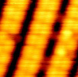
Many physicists believe that halogens–reactive molecules such as and –could be used to treat semiconductor surfaces and improve their performance in microchips. To study the atomic-scale interactions of halogens with and , Andrew Kummel and his colleagues at the University of California at San Diego have used a scanning tunneling microscope. The surface, in one of its configurations, consists entirely of rows of As dimers separated by trenches which expose the all- second layer. In their early experiments treating this surface with a beam, the team was puzzled for weeks because their images showed apparently clean surfaces, with no Br atoms bound–until the day team member Yong Liu adjusted the contrast. That adjustment revealed that the Br atoms were hidden in the darker trenches, bound to Ga atoms in the second layer. “We all looked at each other and felt like absolute idiots,” recalls Kummel.
But the unexpected behavior has a simple explanation, according to their PRL paper. The molecules have easily-donated “antibonding” electrons, and the atoms line the trench walls with empty dangling bonds that easily accept electrons–a perfect match. A top layer As atom, on the other hand, offers only a filled dangling band–one that already contains two electrons. The atoms in a molecule that hits the surface cannot easily bind to As atoms, and they’re quickly attracted to Ga atoms. Kummel and his colleagues present images that show bright rows of As dimers on the surface separated by dark trenches where atoms can be seen bound to second layer atoms.
“It’s very significant that he’s seen these types of reactions,” says Jory Yarmoff, of the University of California at Riverside. As physicists and engineers work toward more intricate processing of semiconductor materials for advanced electronics, atomic-scale effects become more important, and this work suggests that chemical reactions sometimes dominate over the more obvious influences of structure, he says. Although theorists have predicted such effects, this is the first direct observation, and Yarmoff says it could even be used to an advantage in the future. “If you understand the chemistry, you can actually use the chemistry to produce structure on the nanoscale.”