Guided Light Ripples Revealed
Photons outclass electrons for efficient processing of many types of signals. So optical fibers are replacing copper cables, and researchers are furiously designing new types of optical processing elements that could replace much of today’s telecommunications electronics. A new tool, described in the 10 July PRL, should help in the effort. It gives high-resolution images of the optical wave fronts (phase of the waves) inside microscopic optical structures, whereas past techniques mapped only the intensity of the light. The phase data revealed an unexpected phenomenon: “Singularities” show up where two or more different wavelengths interfere within a waveguide. The tool should aid in the design and theoretical analysis of so-called photonic structures because it provides new details on the behavior of light waves within them.
For the past several years physicists have been using photon scanning tunneling microscopes (PSTMs), with increasing sophistication, to map the intensity of light traveling inside optical structures. The PSTM uses a 50-nm diameter optical fiber maintained within 20 nm of a surface to detect the few photons that leak out (the “evanescent field”) as light runs through shallow structures on a surface. The “tunneling” of these photons into the fiber is similar to the tunneling of electrons into the sharp tip of a scanning tunneling microscope, which can map a surface’s atomic-scale hills and valleys. The technique is also similar to near field scanning optical microscopy (NSOM).
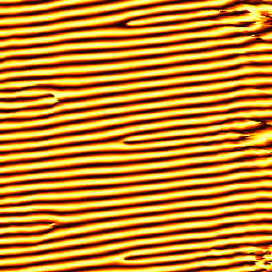
As researchers develop “light on a chip,” they need such tools to evaluate their accuracy in guiding light through a device. “If it doesn’t work, it’s very hard to figure out where it went wrong” without the PSTM, says Kobus Kuipers of the University of Twente in the Netherlands. He is part of a team that has now improved on the PSTM by mapping the phase of the light along an optical channel waveguide–a four-nanometer-high, 3-µm-wide “ridge” of on a surface. They divided their red laser light into two parts: One part went through the waveguide, while the other was used as a reference to be combined with the light picked up by the PSTM fiber, which was moved along and across the waveguide. The interference of the two waves led to images showing the phase of the light in the channel waveguide, which in the simplest case looked like the parallel lines of ripples on water. With the same system the researchers could also map the intensity of light in the waveguide.
When the team manipulated the light to allow two modes with slightly different wavelengths to coexist in the channel, they saw phase singularities in the ripples. These were points where two consecutive wave peaks along one edge of the waveguide merged into a single peak along the other edge. The team reproduced the phenomenon in computer simulations, after they realized what it was, but it had never been observed before. Kuipers says the effect demonstrates that the new system allows more detailed analysis of the light in such structures, because each mode can be tracked independently. That isn’t possible with intensity imaging alone.
The research world is just beginning to come up with photonic devices that could be useful for telecommunications, according to Edwin Thomas of MIT, and tools that allow designers to follow light through their new devices will be critical. “I think there’s going to be lots of surprises” as the imperfections inherent in real materials distort the theoretically expected behavior. Kuipers mentions one more motivation for his technique: “It just gives us a thrill as physicists to see light propagating with all its wave character.”
More Information
Response to this paper: Phys. Rev. Lett. 87, 259401 (17 December 2001).