Scanning Probe Gets Beneath the Surface
For almost two decades, scanning probe microscopy (SPM) has revealed surface features of solid samples in stunning, atomic-scale detail. Although this technique has been a boon to condensed matter and materials science research, it has been limited to surface studies, shedding little light on a solid material’s inner structure. That limitation has now been overcome. In the 25 September PRL, a German physicist demonstrates an extension of SPM to volume imaging–an advance that may have broad applications in both the electronics and materials industries.
Robert Magerle, of the University of Bayreuth in Germany, says the basic idea for his “nanotomography” is to scan the surface of an object in serial fashion, stripping away the sample, layer by layer, and scanning the remaining material at each stage. He compares the approach to “excavation on a nanometer scale.” A computer adds up the two-dimensional images from individual scans to create a composite three-dimensional picture of the object. “No other volume imaging technique available today can achieve nanometer-scale resolution in such a simple and direct way,” Magerle claims.
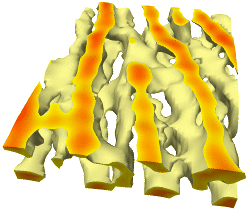
To demonstrate the concept, he took a synthetic rubber material called a block copolymer, imaged its surface, “eroded” it with a beam of oxygen atoms, and imaged it again in 12 more steps, each time removing a 100-nm-thick layer from the surface. The three-dimensional structure of the sample was determined with a resolution of10 nm–a record for volume imaging in a simple bench top experiment, according to Magerle. What’s more, the technique yielded new structural insights. While it was known that the rubber consists of two kinds of polymers (polystyrene and polybutadiene) that reside in separate cylindrical-shaped domains, it was not known how the cylinders link to one another. Close inspection showed that one polystyrene cylinder was connected to four other cylinders–a feature that was not evident from surface views. This result, says Magerle, shows that “volume imaging with SPM offers new information about structures on the nanometer scale that would be difficult, if not impossible, to obtain with existing techniques.”
Nanotomography has several advantages, he says. It provides higher spatial resolution than secondary ion mass spectroscopy, a similar approach, especially when studying rough samples. Another competing method, volume imaging through transmission electron microscopy, is limited to materials that are transparent to electrons and can be cut into uniform slices about 50 nm thick. That rules out hard materials–such as metals, crystals, semiconductors, and ceramics–that are not readily sectioned into thin slices.
Magerle’s method also lends itself to full automation, since separate automated machines can already do etching or SPM. A nanotomography device might identify, for example, structural defects in transistors that hadn’t been seen before. Designers in the polymers industry could use the technique to examine the internal structure of plastics in an effort to optimize their properties.
For specific applications, says Princeton University’s Christopher Harrison, “this approach may be quicker, cheaper, and more straightforward than competing methods.” Sample preparation is fast, and pictures can be interpreted with less ambiguity, Harrison adds. “The combination of SPM and etching techniques should support novel observations, while opening up new avenues for discovery.”
–Steve Nadis
Steve Nadis is a freelance science writer based in Cambridge, MA.