The Most Accurate Defect Measurement
Fault lines between pure crystals affect conductivity in superconductors and the properties of semiconductors in computer chips, so researchers are keen to measure them precisely. A new technique, reported in the 11 December PRL, uses an electron beam to measure so-called stacking faults to an accuracy of a trillionth of a meter (1 pm), ten times better than previous techniques. Taking advantage of the purity of a coherent electron beam, the authors detected the interference of electrons transmitted through large regions of pure crystal on each side of the defect. The technique may improve understanding of crystal interfaces and their relationship with material properties.
Conventional electron microscopes use incoherent beams, usually created by heating a filament, so the electron waves originating from different parts of the filament are not synchronized. But coherent beams come from a sharp tungsten tip from which the electrons are liberated by an electric field. The waves line up more coherently from such a source, just as light streaming through a pinhole in a screen is more coherent than that of a lightbulb. Coherent electron microscopes have become commercially available in just the past five years or so, but they are still quite expensive.
With improvements in coherent electron sources has come a series of new, more precise techniques for measuring material structures. The latest system, developed by Yimei Zhu and his colleagues at Brookhaven National Laboratory in Upton, NY, uses one of the best electron microscopes in the world, but the machine acts more like a ruler than a camera in this case, since the measurement does not involve creating an image.
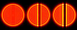
To make the measurement, Zhu and his colleagues first used conventional electron microscopy to find a stacking fault in an otherwise high quality, thin crystal of a high temperature superconductor They then lined up the fault with the center of their electron beam and focused it at a point 160 µm in front of the sample, which created a “shadow image” behind the crystal. That image included a large number of diffraction spots, similar to those created in x-ray crystallography, except that each spot consisted of a striped disk containing oscillating wave interference patterns. The electron waves traveling through the left side of the fault interfere with those traveling through the slightly offset crystal structure on the right side, which leads to the interference patterns.
Thanks to the coherent beam, the team was able to resolve interference patterns out to the 31st disk from the center (“31st order reflection”). By comparing the data with computer simulations, they determined that the space between crystal planes at one of the faults was 0.319 nm shorter than the normal spacing, to an accuracy of 0.001 nm –about 1/100 of the width of a small atom. By comparison, the best electron microscopy can image stacking faults with a resolution of about 0.16 nm, although it gives an image of the atoms as well. Zhu points out that he has used both techniques on the same sample with the same machine.
“It’s a very nice application,” says John Cowley of Arizona State University (ASU) in Tempe, but he cautions that the technique is somewhat specialized: “You can’t look at any old crystal with any old defect in it.” But Stephen Pennycook says the technique might be generalized to include other defect types. The method should help researchers relate interface structures with their effects on material properties, says John Spence of ASU. “A very nice idea.”