The Antimatter Microscope
Matter and antimatter just don’t mix, so it’s surprising that you can probe one with the other. A paper in the 6 August print issue of PRL reports the first results of a new microscope that uses positrons (anti-electrons) to create an image of a surface. The paper shows that positrons can see defects better than either optical or electron beam microscopes. Positrons also provide information about the type of defect present. The scanning positron microscope (SPM) may soon be available as a powerful tool for probing many different materials.
Werner Triftshäuser and his colleagues at the Military University in Munich, Germany, thought positrons might give high quality images of the defects in semiconductor surfaces. Because of their positive charge, positrons are drawn to so-called vacancies, locations within a crystal–or on its surface–where a positively charged nucleus is missing. Without the nucleus, there are fewer electrons in the neighborhood, so a positron can survive longer before colliding and annihilating with its electron counterpart. By measuring a positron’s survival time inside a section of material, the researchers believed they could achieve unprecedented sensitivity to defects. “Positrons can detect defect concentrations of 1 part per million,” according to calculations, says Triftshäuser. “No other method is that sensitive.”
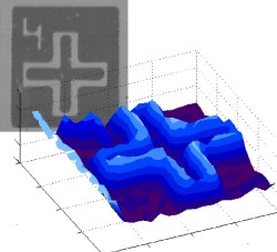
The group placed a silicon wafer etched with a simple pattern of defects inside the chamber of their microscope. They began by scanning the surface with electrons to create an image of the pattern, a procedure similar to that for a standard electron microscope. Then they selected the most interesting regions of the surface to probe with positrons. The positrons, which came from a radioactive sodium source, passed through a series of electric fields that homogenized their energies and bunched them into short pulses. They then passed through another series of fields that accelerated the pulse to a specified energy before focusing it into a 2-µm dot on the silicon surface. By measuring the time between the pulse and the photon flash of electron-positron annihilation the team was able to map the defect regions. They found that positrons that lodged inside defects avoided annihilation for twice as long as those in others regions. By scanning the beam across the surface, they created an image of the defect pattern in the wafer.
The SPM can also give information on the type of defect–information that no other technique can provide, according to Triftshäuser. A positron survives for different lengths of time inside different kinds of defects, so by analyzing a spectrum of positron lifetimes, you can determine the types of defects present in a material, he says. The lifetime measurement also gives unprecedented sensitivity, says Yanching Jean of the University of Missouri in Kansas City. “The lifetime can tell you about defects on the order of an angstrom,” he says, while electrons are sensitive to only about a micron. Alexander Weiss of the University of Texas at Arlington adds that this device is promising for the semiconductor industry, where careful control of defects allows companies to build smaller, better microchips.
–Geoff Brumfiel