Sizing up domain walls in bilayer graphene
A material of interest for the next generation of electronic devices is “few-layer graphene,” a stack of a small number of graphene sheets. From an industrial perspective, preparing few-layer graphene by thermally decomposing silicon carbide (SiC) may be the easiest method for making carbon devices on a large scale. Unfortunately, the mobility of charge carriers in graphene prepared in this way appears to be lower than that in free-standing graphene. Therefore, the mass production of reliable electronic components requires a thorough understanding of what limits the mobility, and how to alleviate it.
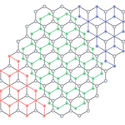
In a paper appearing in Physical Review B, Hiroki Hibino and colleagues at NTT Corporation, in collaboration with Kyushu University, both in Japan, show that bilayer graphene grown on SiC forms two types of structural domains, differing by a 180° rotation. Three types of domain boundaries, with structures intermediate to those of the domains themselves, are attributed to “shifted stacking” of the layers. Hibino et al. propose that roughness at the SiC surface promotes lattice mismatch between adjacent graphene layers, causing strain and thus the stacking domains.
Although more work is needed to uncover the details of the epitaxial growth of graphene, and the precise effects of domain boundaries on its electronic transport, the results of Hibino et al. should steer future efforts in a productive direction. – Matthew Eager