Graphene gets the hole thing
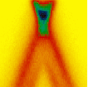
The applicability of a new material for microelectronics depends on how well one can fine-tune the transport properties of its charge carriers. In a paper appearing in Physical Review Letters, Shuyun Zhou and colleagues from the University of California, Berkeley and Lawrence Berkeley National Laboratory use the tools of angle-resolved photoemission spectroscopy to demonstrate they can induce a reversible metal-insulator transition in epitaxial graphene with chemical doping.
The authors study single- and bilayer graphene grown on silicon carbide substrates, since this type of epitaxially grown graphene may have superior device performance compared to graphene sheets that are “peeled” from bulk graphite. The graphene layers are exposed to gas, which dopes the graphene layers with holes and pushes the Fermi energy within the gap between the conductance and valence bands, turning the graphene from a metal into an insulator [1]. With sufficient photon flux, the will desorb and the graphene will revert to being a metal.
This sort of control over transport properties opens possibilities to use expitaxially grown graphene for sensitive microelectronics, while also addressing the physics of hole-doping. – Sami Mitra
[1] K. Novoselov, Nature Mater. 6, 720 (2007).