Sensing Magnetic Fields with a Giant Quantum Wave
Microscopes make small things visible, unveiling fascinating details of nature that would otherwise be hidden. A new microscope reported by Benjamin Lev and colleagues at Stanford University, California, takes this idea to a new level [1]. The team employs a quantum gas of ultracold atoms to map static (dc) magnetic fields at a material’s surface on a microscopic scale, with record field sensitivity, and over a wide temperature range. The field sensitivity of their scanning quantum cryogenic atom microscope, or SQCRAMscope, could be used to unveil the strength and spatial distribution of microscopic currents in a variety of samples. This information would help in the characterization and understanding of unconventional superconductors, strongly correlated materials, and topological materials.
Measurements of small magnetic fields with high resolution are important in many areas of science. They are used, for example, to investigate activity in the brain and heart, for archeological surveys on land and in the sea, and to characterize metal components and their defects. Over the last decade, superconducting quantum interference devices (SQUIDs) have become the “gold standard” for magnetic-field sensing [2, 3]. However, these high-resolution and ultrasensitive magnetometers must be contained in a cryogenic environment, and their exceptional sensitivity is limited to oscillating (ac) magnetic fields. More recently, researchers have realized sensitive ac magnetic-field sensors based on nitrogen-vacancy (NV) defects in diamond [4]. These atom-sized sensors can be used in both room-temperature and cryogenic environments and are unsurpassed in their spatial resolution of roughly a few nanometers.
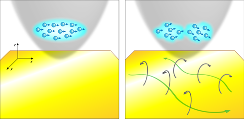
Magnetometers based on atom gases have advanced a lot in the last decade. In this category, vapor-cell magnetometers, which detect magnetic-field-induced shifts in the optical spectrum of a gas, have the highest sensitivity but have poor spatial resolution [5]. A different approach that researchers have explored, and one that offers potentially high spatial resolution for sensing dc fields, relies on a Bose-Einstein condensate (BEC) of thousands of identical magnetic atoms [6–8]. The extremely cold (submicrokelvin) atoms in a BEC are all in the same quantum state and their wave packets overlap, forming a macroscopic quantum object whose density is described by a single wave function. In a magnetic field, the atoms experience a potential because of the Zeeman effect, an interaction that depends on the magnetic moments of the atoms and the field’s strength. This interaction provides a means both to trap the atoms in a cloud with a smooth density distribution and to levitate it above a chip. It also underlies the principle for field sensing: if a spatially varying field is in the vicinity of the BEC, it will distort the trapping potential and, by extension, fragment the cloud. These perturbations to the cloud can then be imaged and analyzed to obtain a map of the local magnetic field.
Experimental groups have explored many of the components that are needed to make a BEC-based magnetic-field microscope, such as trapping the BEC near a chip, measuring magnetic fields from the BEC’s density distribution, and cryogenically cooling the atom chip. With the SQCRAMscope (Fig. 1), the Lev group has merged all of these capabilities into one useful device and then fully characterized its operational limits [1]. The team uses current-carrying wires embedded in a chip to create a bowl-shaped (harmonic) magnetic trapping potential for a BEC of rubidium-87 atoms, which they position above the surface of the chip. The potential is shallow along its x axis and steep along its y and z axes, resulting in a cigar-shaped BEC that is about 300 micrometers long and a few micrometers wide. The microscope is designed such that a sample can be inserted roughly a micrometer below the BEC and scanned laterally (in the x and y directions). The entire apparatus is contained in ultrahigh vacuum to minimize the exchange of heat between the sample and the BEC.
To test and characterize their microscope, Lev and colleagues used the currents from a micropatterned gold sheet: The currents induce density variations along the long direction of the BEC, which the team imaged with a resolution of 2 micrometers using a CCD camera. They then analyzed this “absorption image” to reconstruct the shape of the total local magnetic field. By repeating the experiment at different lateral positions, the team obtained a two-dimensional map of the magnetic field from the sheet. Applying the Biot-Savart law relating magnetic fields to currents and knowing the distance from the BEC to the sheet, the researchers were able to retrieve the current-density distribution in the gold.
Previous cold-atom scanning-probe experiments had to scan the cloud to obtain a spatial map of magnetic fields [7, 9, 10]. With the SQCRAMscope, the surface under study is scanned and the cloud is held fixed. This has the advantage of keeping the atomic cloud the same for each measurement, which facilitates the analysis of the CCD images. Moreover, the Lev group’s version of the microscope is the first to take full advantage of the suppressed density fluctuations in a BEC to achieve quantum-noise-limited sensitivity.
The team reports field sensitivities for the microscope in the region of a few and flux sensitivities of , where is the quantum of flux, or about webers. This latter figure is about 2–3 orders of magnitude better than that of SQUIDs, NV centers, or other state-of-the-art magnetometers, which achieve comparable sensitivities only for ac magnetic fields. The new microscope thus fills a gap for sensitive detection at dc fields. Lev and colleagues also demonstrated that they can analyze samples from room temperature down to 35 K, with 4 K a reasonable goal for the future.
The SQCRAMscope’s features make it well suited for a number of material studies. For one, the device could detect domain walls in magnetic materials or the fields in colossal magnetoresistive systems, which are important for data-storage devices. Another possibility is investigating charge-transport phenomena in strongly correlated and topological materials, which can exhibit quantum effects even at room temperature; this behavior is, for example, expected in artificial honeycomb crystals that host topologically protected states. Finally, Lev and colleagues highlight the possibility of using the magnetometer to search for the so-far undetected current loops that are predicted by certain theories of high-temperature superconductivity.
This research is published in Physical Review Applied.
References
- F. Yang, A. J. Kollar, S. F. Taylor, R. W. Turner, and B. L. Lev, “A Scanning Quantum Cryogenic Atom Microscope,” Phys. Rev. Applied 7, 034026 (2017).
- D. Vasyukov et al., “A Scanning Superconducting Quantum Interference Device with Single Electron Spin Sensitivity,” Nat. Nanotech. 8, 639 (2013).
- J. R. Kirtley et al., “Scanning SQUID Susceptometers with Sub-Micron Spatial Resolution,” Rev. of Sci. Instrum. 87, 093702 (2016).
- M. S. Grinolds, S. Hong, P. Maletinsky, L. Luan, M. D. Lukin, R. L. Walsworth, and A. Yacoby, “Nanoscale Magnetic Imaging of a Single Electron Spin Under Ambient Conditions,” Nat. Phys. 9, 215 (2013).
- B. Patton, E. Zhivun, D. C. Hovde, and D. Budker, “All-Optical Vector Atomic Magnetometer,” Phys. Rev. Lett. 113, 013001 (2014).
- J. Estève, C. Aussibal, T. Schumm, C. Figl, D. Mailly, I. Bouchoule, C. I. Westbrook, and A. Aspect, “Role of Wire Imperfections in Micromagnetic Traps for Atoms,” Phys. Rev. A 70, 043629 (2004).
- S. Wildermuth, S. Hofferberth, I. Lesanovsky, E. Haller, L. M. Andersson, S. Groth, I. Bar-Joseph, P. Krüger, and J. Schmiedmayer, “Bose–Einstein Condensates: Microscopic Magnetic-Field Imaging,” Nature 435, 440 (2005).
- A. Günther, M. Kemmler, S. Kraft, C. J. Vale, C. Zimmermann, and J. Fortágh, “Combined Chips for Atom Optics,” Phys. Rev. A 71, 063619 (2005).
- M. Gierling, P. Schneeweiss, G. Visanescu, P. Federsel, M. Häffner, D. P. Kern, T. E. Judd, A. Günther, and J. Fortágh, “Cold-Atom Scanning Probe Microscopy,” Nat. Nanotech. 6, 446 (2011).
- C. F. Ockeloen, R. Schmied, M. F. Riedel, and P. Treutlein, “Quantum Metrology with a Scanning Probe Atom Interferometer,” Phys. Rev. Lett. 111, 143001 (2013).


