Small Space Makes a Strong Electric Field
Getting photons to interact generally requires extreme conditions—sending them through a dense cloud of ultracold atoms or using super-intense laser light, for example. But now researchers have shown theoretically that photons can be made to interact using very weak light in an ordinary slab of silicon by cutting a precise series of air spaces within the material. The effect could simplify the development of photon-based computing devices, either classical or quantum, using ordinary materials.
In vacuum or air, two light waves will pass through one another, since photons do not interact. In a nonmetallic solid such as silicon, photons can interact through the so-called Kerr effect—the presence of one photon changes the material’s index of refraction, altering how a second photon behaves within it. Photonic interactions within materials would be useful for making photon-based logic gates—the components of an optical computer—yet the Kerr effect usually requires extremely strong electric fields produced by intense laser beams.
But now Hyongrak Choi, Mikkel Heuck, and Dirk Englund of the Massachusetts Institute of Technology, Cambridge, have shown theoretically that similarly strong fields can also be realized by introducing a precise pattern of air spaces in the material. With modern fabrication technology, they suggest, it should be possible to achieve photon interactions even with very weak light.
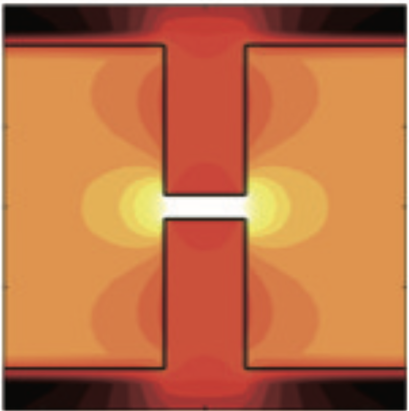
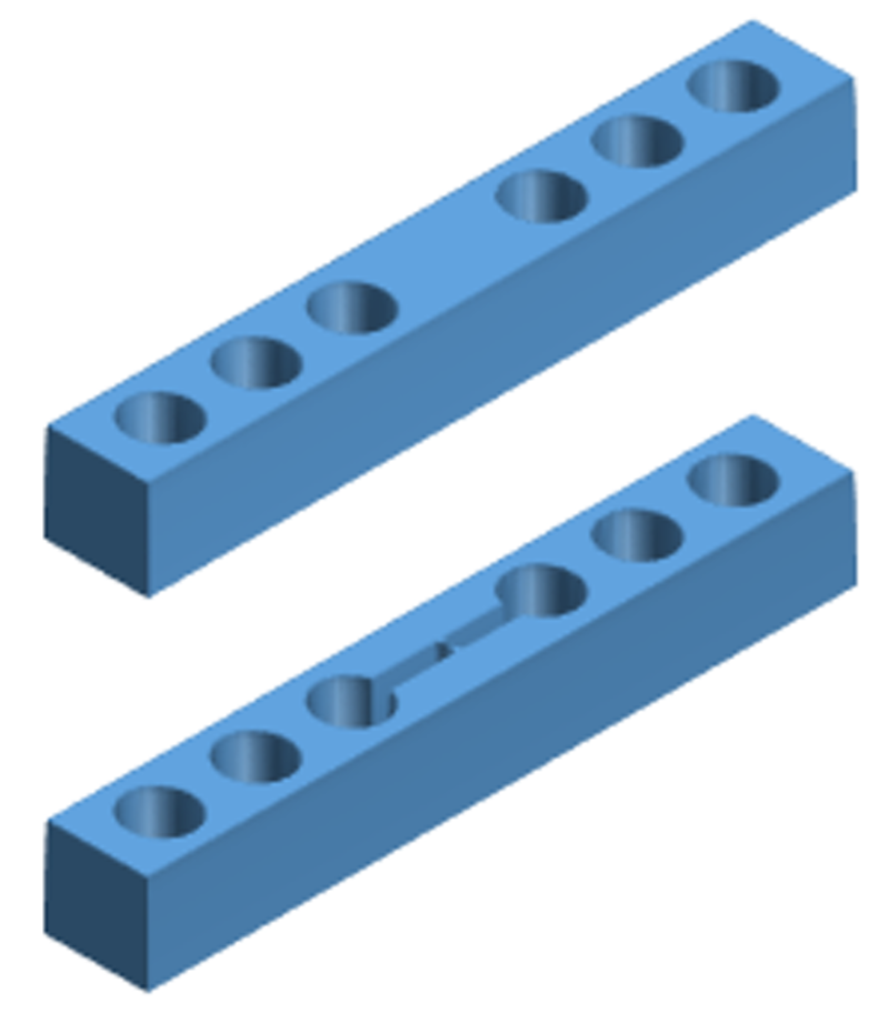
The team’s work builds on that of Michal Lipson of Columbia University in New York and her colleagues, who, in 2005, studied light stored in silicon [1]. Imagine a “bar” of silicon of square cross section, about 10 micrometers long, having a series of equally spaced, horizontal holes drilled through it, each one almost as wide as the bar. To make an optical cavity, researchers skip the center hole, leaving a solid region in which light can become trapped. Lipson and her colleagues showed theoretically that cutting a narrow, horizontal slot through the center of the cavity, connecting the holes at either end, could boost the maximum strength of the electric field of the trapped light by concentrating the light into a small volume. Assuming the electric field is exclusively vertical, this slot boosts the field strength within the gap by about 10 times because of the difference in electromagnetic properties between air and silicon.
Choi and colleagues show that modifications of this simple air gap can focus the field energy even more. For example, imagine placing a vertical column of silicon across the center of the horizontal gap. The electric field is now parallel to this new silicon-air interface, rather than perpendicular, so the rules for the field are different. Electromagnetic theory requires the field to be identical across the silicon-air interface, so the strong field from the air gap permeates inside the column, or “bridge.” Meanwhile, since an electric field carries 10 times the energy density in silicon as in air, the bridge gives another roughly tenfold increase in maximum energy density.
In computer simulations, the team confirmed these theoretical estimates. Choi and colleagues further argue that one can add smaller copies of the gap/bridge construction onto the original, first putting a secondary horizontal gap within the vertical bridge, and then crossing that gap in turn with another, secondary silicon bridge. This elaboration again boosts the maximum field value and associated energy density. In principle, the procedure can be repeated indefinitely on smaller scales, limited only by material properties and fabrication techniques. For some choices of slot and bridge length scales, the researchers note, in the limit of many such elaborations, the structure becomes simply an air gap into which two sharply pointed peninsulas protrude, just reaching one another. This structure concentrates the field energy into a nanoscale zone near the tips.
“Surprisingly,” says Englund, “we could use geometry alone to strongly concentrate the electromagnetic field inside the cavity.” In calculations, the team also found that this technique could be enough to achieve a strong Kerr effect, even from one photon. That is, injecting a single photon into the cavity would significantly change how a second injected photon would behave, creating an effective interaction between the photons. But achieving this in practice, the team notes, might require filling the slot area with organic materials having enhanced Kerr properties.
“This is remarkable work,” says physicist Mohammad Soltani of Raytheon, who specializes in nanophotonics. “It’s probably the most promising [concept] to date for making practical devices such as photon gates for quantum information processing.”
This research is published in Physical Review Letters.
Editor’s Note (10 July 2017): A similar design for strong field confinement in photonic crystal cavities was published last year. The new work demonstrates that these field enhancements are likely to be sufficient to achieve an ultrastrong Kerr effect, even with just one photon.
–Mark Buchanan
Mark Buchanan is a freelance science writer who splits his time between Abergavenny, UK, and Notre Dame de Courson, France.
References
- J. T. Robinson, C. Manolatou, L. Chen, and M. Lipson, “Ultrasmall Mode Volumes in Dielectric Optical Microcavities,” Phys. Rev. Lett. 95, 143901 (2005).