Taking Temperature in 2D
To build robust electronic devices, it is crucial to know how the components change size in response to heat generated by electric currents. A new experiment demonstrates electron microscopy as a tool for creating a map—with nanometer resolution—of thermal expansion in 2D materials. Observations of 2D carbon and 2D semiconductors showed that the thermal response strongly depends on the number of atomic layers in the material, with single layered materials exhibiting surprisingly large expansion rates. This behavior, which the researchers have yet to fully explain, will need to be accounted for as engineers develop next-generation nanoelectronic devices relying on 2D materials.
Probing the temperature and thermal properties of very small objects has long been a challenge. Conventional thermometers are simply too large: they would alter the temperature of the target object if they were placed in contact with it. Researchers have developed less invasive techniques that use a sharp probe with sensors that can measure the heat flow between the object and the probe. Other methods record temperature by detecting light emitted by (or reflected from) the object. But such techniques cannot provide sufficient spatial resolution for studies of transistors and other components in future nanoscale devices.
Recent work has shown that scanning transmission electron microscopy (STEM) can measure temperature with nanometer spatial resolution [1]. The technique involves measuring the amount of kinetic energy lost by electrons passing through a material, a quantity that is temperature dependent. Robert Klie and his colleagues from the University of Illinois at Chicago have adapted this STEM method to the case of measuring thermal expansion in 2D materials.
The team investigated graphene (2D carbon) and several transition metal dichalcogenides (TMDs), which are 2D semiconductors with unusual electronic properties. They fabricated small flakes of various thicknesses and placed them on a heated mesh, which allowed the temperature of the samples to be controlled.
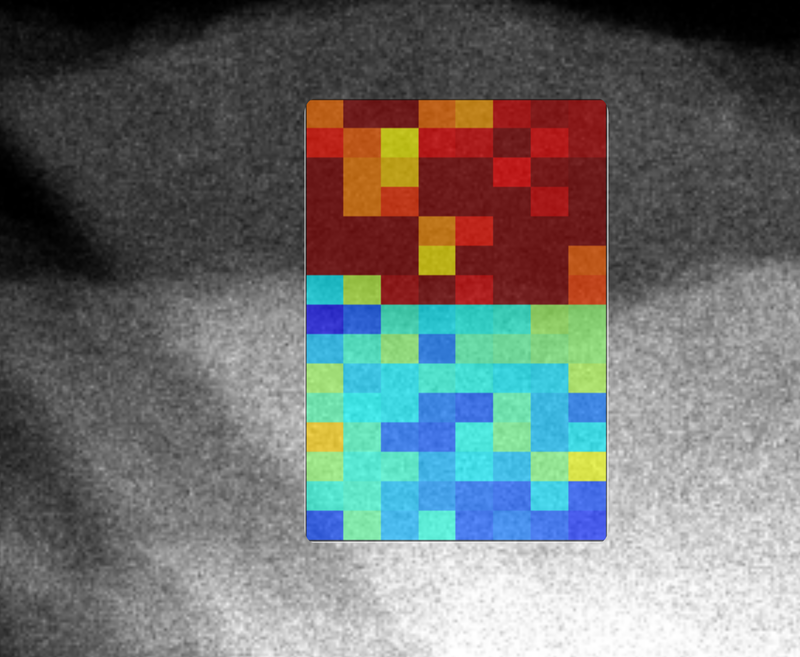
For the STEM measurements, the researchers scanned an electron beam across each sample and recorded the energy of transmitted electrons. They produced, at each location, a spectrum of energy lost through interactions with the sample. One of the main loss mechanisms is the excitation of plasmons, which are “collective oscillations of electrons in a material,” Klie explains. The energy of the plasmons depends on the wavelength of these collective oscillations, which in turn depends on the volume occupied by the electrons. So you can measure changes in the volume of the material by measuring the energy of the plasmon peak.
Klie and his colleagues recorded the position of the plasmon peak at various temperatures between 373K and 723K . As temperature increased, the peak shifted, reflecting a change in volume. The researchers used the shift to calculate the thermal expansion coefficient, which is the fractional volume change per degree of temperature increase. They found that this coefficient strongly depended on the number of atomic layers in the sample. For the TMDs, the expansion rate increased—in some cases by a factor of 45—when the number of layers decreased from four to one. For graphene, which experiences contraction rather than expansion when heated, the coefficient for a monolayer was 30 times that of samples with four or more layers. This behavior suggests that single layers respond more strongly to temperature changes because they are not constrained by interlayer interactions. However, these interactions are normally weak in 2D materials, so a more sophisticated model may be needed to explain why the expansion of multiple layers is so different from that of single layers, says Klie.
The team produced maps of the thermal expansion coefficient with spatial resolution of around 2 nanometers. Klie says that such maps could help in designing nanoelectromechanical systems with connections between different 2D materials. By observing how the thermal expansion varies across boundaries between different materials, engineers can avoid structural failure by adjusting the geometry or the type of materials used.
“Measuring the thermal expansion coefficient in 2D materials is useful for materials engineering,” says electron microscopy expert Matthew Mecklenburg from the University of Southern California. He is surprised by the dramatic increase observed in the thermal expansion coefficient as the number of layers decreases. For single layers, the expansion data suggests that 2D materials behave more like plastics than metals—an unexpected result that Mecklenburg would like to see verified.
This research is published in Physical Review Letters.
–Michael Schirber
Michael Schirber is a Corresponding Editor for Physics Magazine based in Lyon, France.
References
- M. Mecklenburg, W. A. Hubbard, E. R. White, R. Dhall, S. B. Cronin, S. Aloni, and B. C. Regan, “Nanoscale Temperature Mapping in Operating Microelectronic Devices,” Science 347, 629 (2015).