Image—The Real Deal on 2D Electron Motion
One way to study how electrons move in materials is to limit their motion to two dimensions along the interface between two semiconductor crystals (like an “ant farm” for electrons). Now Richard Steinacher of the Swiss Federal Institute of Technology (ETH) in Zurich and his colleagues have improved a technique for imaging these so-called two-dimensional electron gases (2DEGs). Their system can display the intrinsic conduction patterns of electrons and separate them from the effects of the probe.
The scanning gate microscopy technique involves sending a current through a 2D system and recording how that current changes as a needle-like probe scans over the image region. The probe acts as an obstacle to electrons—with a voltage that deflects or even repels them—and this “detouring” affects the amount of current measured in the 2D structure. Each point is then colored based on the current measured when the probe was at that position. This signal is strongest when the probe touches regions with high densities of electrons.
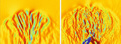
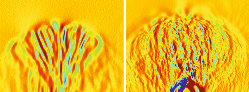
Ordinarily, the probe voltage needs to be so high that it distorts the image. Steinacher and his colleagues have managed to produce images over a wide range of voltages, from “weakly invasive” (left in the image) to “strongly invasive” (right). Analyzing this wide range of conditions provides details of the probe’s interactions and other properties of the 2DEG. With the probe-induced distortions removed, effects such as electron wave interference patterns become more visible.
This research is published in Physical Review B.
–David Ehrenstein
David Ehrenstein is a Senior Editor for Physics Magazine.


