Universal Scaling Laws for 2D Schottky Diodes
Photodetectors, electrical switches, solar cells, and other devices based on 2D materials rely on Schottky diodes, which are metal-semiconductor junctions that force electrical current to flow in one direction. To design, model, and optimize these 2D devices, researchers need to know the mathematical relationships, or scaling laws, between the device’s transport properties and temperature. But not having found such laws for 2D Schottky diodes, many researchers have applied 3D scaling laws inappropriately. Now, Yee Sin Ang and colleagues at the Singapore University of Technology and Design have identified universal scaling laws for different configurations of Schottky diodes based on 2D materials.
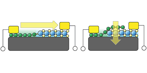
To find the scaling laws, they developed a mathematical model of metallic 2D materials that expresses the energy-momentum relation and the electronic density of states for the metal in highly generalized forms. This allowed them to analytically extract relationships between an electrical current in a Schottky diode and temperature, which can be described in terms of a power scaling law. For lateral Schottky structures, where the metal and semiconductor come in contact along their edges, the scaling exponent is 3/2. For vertical structures, where the two materials are stacked atop one another, the exponent is 1.
These specialized scaling laws for vertical and lateral structures could allow researchers to be more specific with their modeling and device optimization, depending on the type of contact configuration. While the researchers focused on graphene-based heterostructures, they note that the scaling laws can also be applied to a broad range of 2D systems, including semiconductor quantum wells, spintronic systems, transition-metal dichalcogenides, and thin films of topological solids.
This research is published in Physical Review Letters.
–Michelle Hampson
Michelle Hampson is a freelance writer based in Toronto.