Device Acts as Both Solar Cell and Battery
Photoelectric devices, which convert light energy into electricity, have a vital role in clean energy technologies. They often need to be coupled to batteries that store the captured energy, but researchers have now built a device that combines photoelectric charge generation with charge storage. The excited electrons can be retained for at least a week, until they are discharged as an electric current. The team says the device might find uses in energy generation, photodetectors, or light-based memories.
A good photoelectric device contributes a charge carrier to an electric current nearly every time it absorbs a photon; in other words, it has a high “external quantum efficiency” (EQE). The problem is that the negatively charged electron and the positively charged hole generated by a photon often recombine shortly after their creation. One way to increase the EQE of a device is to temporarily trap the charge carriers—at crystal defects, for example—before recombination can occur.
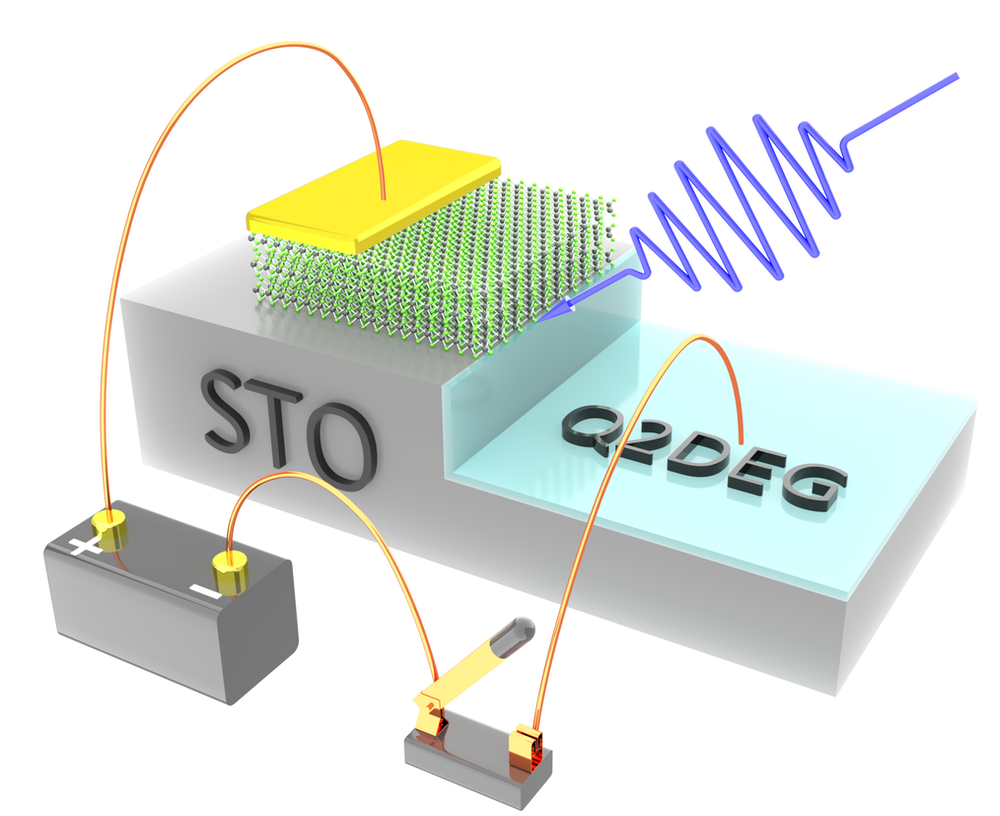
Yucheng Jiang of the Suzhou University of Science and Technology, China, and his co-workers set out to use this strategy in a device called a van der Waals heterojunction, in which two materials are held in contact by relatively weak van der Waals interactions [1]. They used tungsten diselenide, a semiconducting material, and the transparent conductor strontium titanium oxide (STO). On the surface of the STO, the team produced a nearly two-dimensional “electron gas” (a state in which electrons move freely and independently) by employing a surface treatment. Using an electron gas as one component of such a heterojunction was new and led to the device’s novel properties.
The interface region between the two materials forms a so-called p-n junction, a common structure in solar cells. Ordinarily, photons generate electron-hole pairs that can be separated by a voltage, though some inevitably recombine. Jiang and colleagues hoped that in their structure, recombination might happen more slowly than in other p-n photovoltaic devices. But to their surprise, they found that the photoinduced charge carriers could persist for very long times. After illuminating their device with a blue laser and then storing it in the dark at a temperature of 30 K for up to 7 days, they could extract a large current (2.9 milliamps) when they connected it to a circuit. The photoexcited charge was being stored without degrading appreciably, as if in a battery that could be charged and discharged at will. They named this new phenomenon chargeable photoconductivity.
The researchers think that the trapping happens in a part of the tungsten diselenide film called the space-charge region, adjacent to the interface with the STO crystal. Here, light-induced holes can be accumulated and retained until a sufficiently large applied voltage draws them into a circuit. The device is then ready to be charged again by light. The EQE of the device is 93.8%, whereas many photovoltaic cells are considered “high performance” if their EQE is greater than 50%. However, the need to cool the device to around 30 K to keep the stored charge stable might restrict it to certain applications, Jiang says, unless improvements using other materials can significantly raise this operating temperature.
The heterojunction device could also act as an optical memory. Information would be input with a light pulse and stored until it was read out as a pulse of electric current. “We do not know what the limit of this stability is, but we think the storage lifetime is almost infinite,” Jiang says.
Other layered materials have previously been used to make heterojunction devices with a photoinduced storage capability [2, 3]. But Jiang says that the trapping process in those cases is less readily switched on and off because it involves “stronger” traps (in defect sites in the crystal).
Materials engineer Zhimei Sun of Beihang University in China says that the observed effect could prove important, but he would need to see more data to be convinced that the researchers fully understand the mechanism.
The paper “suggests a novel device structure for photoelectric conversion and storage,” says Mark Hersam of Northwestern University, Illinois, a specialist in low-dimensional nanoelectronic materials. “This type of work is likely to be elaborated further in the future as the field of van der Waals materials increasingly takes advantage of opportunities to form heterostructures” that include many other types of materials, he says.
–Phillip Ball
Philip Ball is a freelance science writer in London. His latest book is How Life Works (Picador, 2024).
References
- Y. Jiang et al., “Coexistence of photoelectric conversion and storage in van der Waals heterojunctions,” Phys. Rev. Lett. 127, 217401 (2021).
- K. Roy et al., “Graphene–MoS2 hybrid structures for multifunctional photoresponsive memory devices,” Nat. Nanotechnol. 8, 826 (2013).
- D. Xiang et al., “Two-dimensional multibit optoelectronic memory with broadband spectrum distinction,” Nat. Commun. 9, 2966 (2018).


