Shining Light on Electron Microscopy
Electron microscopy reveals structure from the submicron to the atomic length scale. The technology has already given us so much beautiful imagery, including pictures of microscopic creatures and nanorobots, as well as movies of traveling atomic dislocations. And yet the microscopic world offers much more to explore—after all, “there is plenty of room at the bottom,” as the physicist Richard Feynman famously said. A development by Thomas Juffmann from the University of Vienna and colleagues could open up a new vision of the very small [1]. Using short laser pulses, the researchers controlled the shape of an electron beam, imprinting it with patterns of bars, crescents, and even a smiley face. This programmable electron beam shaping could be used to better focus electrons for ultrafast microscopy or to reduce the electron exposure of easy-to-damage biological samples.
The field of electron microscopy is quite healthy, but focused effort could get it in better shape. The main challenges are that electron microscopes are too blurry, too deadly, and too slow. The blurriness is from aberrations caused by imperfections of the electron lenses. Researchers have made major progress in correcting aberrations, but lens imperfections remain a problem, and quantum decoherence from electrons interacting with the microscope structure may also be limiting the spatial resolution. The deadliness is related to the damage that electrons can impart on a biological sample. It’s true that electron microscopy can be used to image biomolecules—a capability recognized by the 2018 Nobel Prize in Chemistry—but electron microscope images of living and functioning organisms have not been possible, as organisms cannot survive the currently required levels of electron exposure. Finally, the slowness concerns the inability of electron microscopes to capture atomic behavior that happens on attosecond timescales. It should be noted that femtosecond electron microscopy has been around for some time but having both atomic-scale spatial resolution and atomic-scale time resolution is still out of reach.
To tackle these challenges, the field of electron microscopy needs innovative ideas. The work of Juffmann and colleagues is a wonderful example of a potentially disruptive research direction. Their method combines two established electron beam technologies. The first is the extraction of electrons from metal nanotips with femtosecond laser pulses, which was shown in 2006 [2]. The second is the manipulation of the quantum phase of free electrons with laser light, first demonstrated in 2001 [3]. The researchers employ an additional trick, which involves writing a pattern into the laser light.
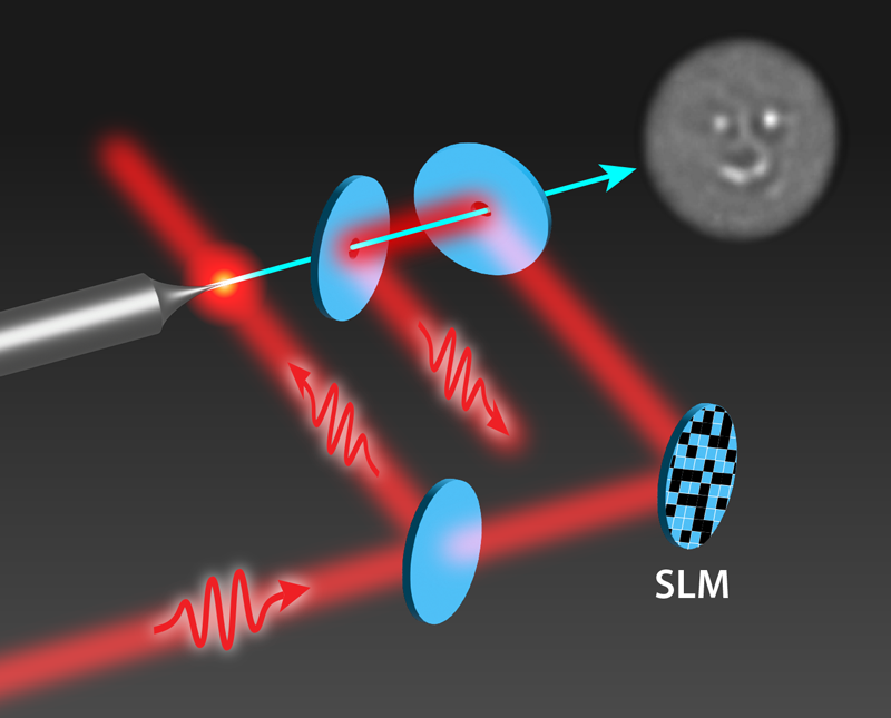
In their experiment, the Juffmann group first fires a laser pulse at a metal tip, where the pulse’s electric field causes a burst of electrons to be emitted straight off the end of the tip (see Fig. 1). With careful timing, the researchers then cross the free electrons with another laser pulse that manipulates the electron beam. The manipulation occurs through a process called stimulated Compton scattering, in which a single electron interacts with two photons in the laser light. This interaction, which was first predicted by Kapitza and Dirac in 1933, changes the phase of the electron, and thus affects its motion.
The Kapitza-Dirac effect is proportional to the number of photons, so the stronger the light is in a certain region of the pulse, the more the electrons are affected in that region. Juffmann and colleagues use this proportionality to shape the electron beam. They place a spatial light modulator in the path of the second laser pulse. The modulator produces intensity variations that manipulate the electrons in a desired, programmable pattern. The researchers demonstrate control of hundreds of “pixels” in the electron beam, allowing them to create intricate patterns, such as a smiley face and a cross. The cross pattern is relevant for addressing astigmatism, which is one of the aberrations in electron microscopy that always needs correction.
What problems can be pursued with the advent of this new technology? It would be exciting to attempt electron ptychography, which is a way of producing images by analyzing the data from multiple exposures of a target [4]. This technique does not use a lens, but it does require a specific control over the input electron beam—something that the new shaping method could provide. The ultimate promise of electron ptychography is that the imaging resolution could be improved. As mentioned, current resolution is limited by uncorrected aberration of lenses and decoherence from interactions with nearby materials in the microscope. Using laser light to manipulate the electron motion avoids both of these issues.
The new technology is also exciting in the context of electron ghost imaging, which was recently demonstrated [5]. In ghost imaging, the object to be imaged is illuminated with a series of preset electron patterns, whose known structure is leveraged to obtain an image from the detected electrons. The potential advantage is that input patterns can be chosen so that the target object is exposed to fewer electrons. The laser manipulation of Juffmann and colleagues affords a means by which to generate the initial patterns with higher spatial resolution than previous electron ghost-imaging techniques. If high-resolution ghost imaging can be combined with new methods of protecting biological cells, such as covering the biological specimen with graphene layers [6], this may bring us closer to the dream of seeing living tissue in an electron microscope.
References
- M. Constantin et al., “Transverse electron-beam shaping with light,” Phys. Rev. X 12, 031043 (2022).
- P. Hommelhoff et al., “Field emission tip as a nanometer source of free electron femtosecond pulses,” Phys. Rev. Lett. 96, 077401 (2006).
- D. L. Freimund et al., “Observation of the Kapitza–Dirac effect,” Nature 413, 142 (2001).
- M. Guizar-Sicairos and P. Thibault, “Ptychography: A solution to the phase problem,” Phys. Today 74, 42 (2021).
- S. Li et al., “Electron ghost imaging,” Phys. Rev. Lett. 121, 114801 (2018).
- K. Koo et al., “Live cell electron microscopy using graphene veils,” Nano Lett. 20, 4708 (2020).