Semiconductors in the Spotlight
Understanding how semiconductors respond to illumination has been crucial to the development of photovoltaics and optical sensors. But some light-induced behaviors have been less thoroughly investigated. For example, when some semiconductors are illuminated, their mechanical properties can change drastically, a phenomenon known as photoelasticity. Photoelastic materials could be useful in the development of flexible electronics, but researchers do not understand in detail the mechanism behind the effect. Now, based on experiments and simulations, Rafael Jaramillo of the Massachusetts Institute of Technology and colleagues present a new theoretical framework that explains photoelasticity in terms of lattice defects [1].
The researchers used a diamond-tipped probe to make nanometer-scale indentations in samples of zinc oxide, zinc sulfide, and cadmium sulfide—first in the dark, and then under a range of visible and ultraviolet wavelengths. All three materials hardened to varying degrees when illuminated, with cadmium sulfide showing the largest and most consistent response. For every sample, the effect increased as the photon energy increased toward the material’s band gap.
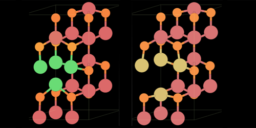
The team then modeled multiple unit cells of each material, looking specifically at the effect of lattice vacancy defects. These defects make the material softer, as they cause atoms in the lattice to experience, on average, less repulsion from their neighbors. Upon illumination, however, atoms around the vacancy site become excited, increasing their mutual repulsion and causing the material to stiffen. Jaramillo and colleagues found that they could tune a material’s illumination response by varying the number of defects in the lattice. They say that their discovery could lead to the identification of materials whose photoelasticity is more pronounced or more easily manipulated.
–Sophia Chen
Sophia Chen is a freelance science writer based in Columbus, Ohio.
References
- J. Dong et al., “Giant and controllable photoplasticity and photoelasticity in compound semiconductors,” Phys. Rev. Lett. 129, 065501 (2022).