Atomic Spreading Produces Novel Superconductors
A type of zero-resistance material called a topological superconductor could lead to error-free quantum computing, but efforts to make such a material have so far come up short. Researchers have now shown that a recently developed fabrication technique that could generate topological superconductors passes a key test [1]. They produced a superconducting layer on top of a topological insulator—a thin sheet of material in which electrical currents are confined to the edges. The technique uses a “seed” of deposited metal that spreads out much like a liquid over the topological insulator’s surface, forming a new crystalline structure. The resulting material exhibits zero resistance, but further tests are needed to determine whether it’s a topological superconductor. Even if it isn’t, the researchers are hopeful that new topological superconductors could be created using the technique.
Many types of materials exhibit topological electronic properties that result from quantum-mechanical phenomena that are relatively insensitive to environmental disturbances. This robustness could lead to fewer errors in computations performed with topological superconductors, whose electrons are expected to form collective quantum states that could potentially be used for quantum bits (qubits). Various attempts to produce topological superconductors have been inconclusive. One technique is to induce superconductivity in a 2D topological material, but so far researchers have succeeded in only a few specific cases, limiting efforts to confirm the presence of topological superconductivity, says Sanfeng Wu from Princeton University.
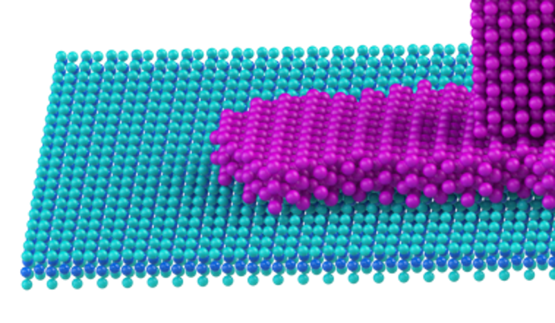
Last year Wu and his colleagues developed what they hope will be a general method for fabricating 2D topological superconductors [2]. The technique involves the infiltration of metal atoms into a thin insulating material. Atomic mixing at interfaces is well known whenever two solids are placed in contact, but the atoms typically diffuse distances of just nanometers, and they do so in a nonuniform way, Wu explains. The researchers discovered that atoms could travel longer distances when they placed a small block of the metal palladium (Pd) on a single layer of the topological insulator tungsten ditelluride (WTe2) and raised the temperature to 200 °C. After about an hour, palladium atoms spread over a region as wide as 10 µm. “It’s like a liquid spreading on a film, which is surprising, since palladium melts at 1500 °C,” Wu says. The infiltrating atoms formed a new crystal structure, Pd7WTe2, that had never been observed before.
The researchers have now confirmed that this new material is superconducting. What’s more, they have explored other materials and have shown that the atom-spreading technique can work with a variety of ingredients. Of special interest is molybdenum ditelluride (MoTe2), as recent experiments showed that a twisted MoTe2 bilayer—a pair of single layers with one slightly rotated with respect to the other—exhibits a rare topological behavior called the fractional quantum anomalous Hall effect [3]. MoTe2 degrades in air, making its integration with other materials very challenging. Using a palladium seed, Wu and his colleagues were able to induce superconductivity in a twisted MoTe2 bilayer that was protected by layers of boron nitride above and below.
The researchers say that their technique offers a highly customizable method of introducing superconductivity into 2D topological materials. The atom spreading can be controlled to form superconducting disks or rings of desired sizes, and the resulting “islands” can be connected with bridges to form devices, such as circuit elements called Josephson junctions that are used in superconducting qubits. “With this technique, we can think of a 2D material as a canvas that we can ‘paint’ devices onto,” says graduate student team member Yanyu Jia. These devices could then be used to explore the properties of the superconducting state, potentially revealing the exotic behavior expected in topological superconductors.
Nanotechnology expert Christian Schönenberger from the University of Basel, Switzerland, says the new work is not fundamentally different from his own team’s recent demonstration of induced superconductivity in WTe2 [4]. But Wu believes that there are key differences between the two experiments, in particular, the larger area coverage that his team observes suggests a new mechanism for the movement of atoms. Materials scientist Yoichi Ando from the University of Cologne, Germany, agrees that a new—and surprising—chemical process seems to be at work. “I think this technique will be of interest to a broad range of researchers working on 2D materials as a new fabrication tool,” Ando says.
“This is a very exciting result,” says Xiaodong Xu from the University of Washington, Seattle, whose team observed the fractional quantum anomalous Hall effect in MoTe2 [3]. He says the new technique promises on-demand fabrication of 2D superconductors. “I can envision many new device structures enabled by this powerful approach,” Xu says. “In fact, my group has already reproduced some of these results after we learned of the work.”
–Michael Schirber
Michael Schirber is a Corresponding Editor for Physics Magazine based in Lyon, France.
References
- Y. Jia et al., “Superconductivity from on-chip metallization on 2D topological chalcogenides,” Phys. Rev. X 14, 021051 (2024).
- Y. Jia et al., “Surface-confined two-dimensional mass transport and crystal growth on monolayer materials,” Nat. Synth. 3, 386 (2023).
- H. Park et al., “Observation of fractionally quantized anomalous Hall effect,” Nature 622, 74 (2023).
- M. Endres et al., “Transparent Josephson junctions in higher-order topological insulator WTe2 via Pd diffusion,” Phys. Rev. Mater. 6 (2022).