Reaching a new resolution standard with electron microscopy
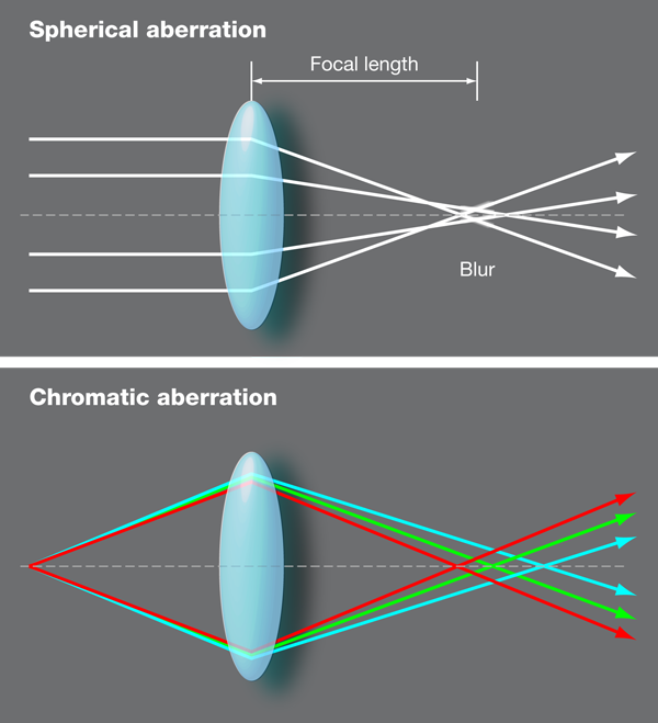
The invention of spherical aberration correctors has been the most significant contribution to the field of transmission electron microscopy since the field emission gun. Chromatic and spherical aberration, well known from optics, also play a role in electron microscopy. Lens aberrations are not unique to the magnetic lenses used in electron microscopes, but rather a fundamental problem of optical systems. Because of spherical aberration, rays entering a round lens system away from the optical axis are refracted more strongly than those entering close to the optical axis (see Fig. 1, top). A similar effect is chromatic aberration, which occurs when rays with different wavelengths enter a round lens, resulting in the rays diffracting differently depending on their wavelength (see Fig. 1, bottom).
Transmission electron microscopes (TEM) and scanning transmission electron microscopes (STEM) equipped with such aberration correctors have been shown to resolve interatomic spacings approaching [1,2] and achieve single-atom sensitivity [3]. To compare, the highest resolution in uncorrected STEM imaging is about at the same electron wavelength [4,5]. Using aberration-corrected TEMs, one can now also perform atomic resolution imaging with longer wavelength electrons, which tend to be less damaging to samples. This is of particular importance for low-dimensional nanostructures, such as nanotubes, metal clusters, or single-layer sheets containing light constituent atoms, such as lithium, boron, or carbon.
One of these novel low-dimensional nanostructures is single-layer hexagonal boron nitride. The hexagonal lattice of boron nitride contains boron and nitrogen atoms separated by a distance of Å. This two-dimensional structure exhibits intriguing magnetic and electronic transport properties different from its monoatomic cousin, graphene. Single-layer boron nitride is also very sensitive to electron beams at energies higher than . One could use beams of lower energy, but a side effect of using electron beam energies as low as is that the chromatic aberrations of the imaging system become more dominant in determining the spatial resolution limit. Even in spherical-aberration-corrected TEMs, the smallest spatial resolution at is limited by the chromatic aberrations of the objective lens [6]. This means that either chromatic aberration correctors or more monochromatic electron sources are needed in order to achieve atomic resolution.
Since the emergence of aberration-correctors and monochromators, the TEM community has been looking for an appropriate benchmark sample to test the resolution and sensitivity of new instruments. In this light, monolayer boron nitride would at first glance appear an unlikely candidate for such resolution tests, since hexagonal boron nitride, in particular, monolayer boron nitride, is highly beam sensitive with a knock-on damage threshold of and for boron and nitrogen atoms, respectively.
In a paper appearing in Physical Review B [7], Nasim Alem, Rolf Erni, Christian Kisielowski, Marta Rossell, Will Gannett, and Alex Zettl at the University of California, Berkeley, and Lawrence Berkeley National Laboratory, both in the US, have demonstrated that their unique setup of using aberration-corrected and monochromated transmission electron microscopy at can image the hexagonal lattice structure of boron nitride, and identify the atomic positions of both boron and nitrogen atoms in single-layer boron nitride. Beyond this milepost in imaging resolution, the group shows they can synthesize TEM samples of hexagonal boron nitride with conventional ex situ preparation techniques, like exfoliation and plasma etching.
In agreement with previous studies [6,8], Alem et al. have shown that vacancies in boron nitride are predominately associated with missing boron atoms in single-layer boron nitride, as well as at the edges of boron nitride sheets. Yet this work goes further than any of the previous studies by showing that the combination of aberration-corrected TEM at with a monochromated electron source can achieve ultrahigh resolution imaging down to single atoms. This opens a new path to quantifying the image resolution and chemical sensitivity in next generation transmission electron microscopy instrumentation.
To explain the significance of this result, let us consider a TEM operating at , where you would have high enough resolution to image boron nitride. Although electrons have a wavelength of about , the spatial resolution of conventional electron microscopy using electrons has so far been limited to about , suggesting that the electron-optical system of the TEM is the predominant limiting factor rather than the availability of short wavelength electrons. Since the spatial resolution is proportional to [9], using instead of in an uncorrected TEM could increase the resolution limit from to more than for the same spherical and chromatic aberrations of the objective lens. Although chromatic and spherical aberrations are the resolution-limiting elements in most optical microscopes, they can often be corrected by designing round lenses with negative aberrations. Unfortunately, it is not possible to design analogous lenses for electron microscopes, which bend electron beams with magnetic fields, creating an effect analogous to refraction [9].
Recently, aberration correctors have become available in state-of-the-art TEMs. These consist of a complex arrangement of quadrupole, hexapole, and octupole magnetic lenses [10,11]. Aberration-corrected electron microscopes have demonstrated that imaging and spectroscopy is now possible with resolutions as high as using or electron sources [1,2,12,13]. Yet even in spherical-aberration-corrected instruments, lowering the electron energy to is limited by the chromatic aberration of the objective lens, or the energy spread in the incoming electron beam . Using single-layer boron nitride, Meyer et al. demonstrated that spherical aberration correction alone cannot achieve atomic resolution at [6]. Since chromatic aberration correctors are not yet commercially available, using a monochromated electron source is the only alternative in high-resolution TEM to minimize the effects of chromatic aberration at low and increase the spatial resolution limit for imaging. However, monochromated electron sources often achieve the desired decrease in by discarding the majority of electrons, resulting in a significant decrease of the image signal. It was therefore not clear that using a monochromator in connection with an aberration corrector would provide an electron beam intense enough for ultrahigh resolution imaging at .
The findings of Alem et al. [7] go beyond the simple identification of atomic species in single-layer boron nitride, they also provide a roadmap to identifying the chemical sensitivity of high-resolution images as a function of sample thickness. The images clearly distinguish the atomic positions of nitrogen and boron in the hexagonal lattice of monolayer boron nitride. As expected, for an even number of boron nitride sheets, the intensity of the atomic columns in the hexagonal rings of boron nitride is identical since each column now contains an alternate stacking of boron and nitrogen atoms (see Fig. 1 in Ref. [7]). While this appears to be trivial, it is of crucial importance to this study, and to the field of aberration-corrected high-resolution TEM. As demonstrated by this work, the intensity of the atomic fringes in an aberration-corrected HRTEM micrograph depends on the atomic mass and thickness of the atomic column, as well as on the orientation of the lattice with respect to the incoming electron beam.
In conclusion, single-layer boron nitride has clearly become the new benchmark test for imaging resolution in aberration-corrected low-energy TEM/STEM [6,8,14]. The hexagonal lattice of boron nitride can, however, only be imaged at by aberration-corrected TEM in connection with either monochromated or chromatic-aberration-corrected TEM. Alem et al. show that monolayer boron nitride samples can be made from boron nitride powders using conventional TEM sample preparation methods and furthermore demonstrate that monolayer boron nitride, beyond its importance for fundamental physics and nanoelectronic applications, can also be used for low aberration-corrected ultrahigh-resolution imaging with single-atom sensitivity.
References
- C. Kisielowski et al., Microsc. Microanal. 14, 469 (2008)
- R. Erni et al., Phys. Rev. Lett. 102, 096101 (2009)
- M. Varela et al., Phys. Rev. Lett. 92, 095502 (2004)
- E. M. James and N. D. Browning, Ultramicroscopy 78, 125 (1999)
- E. M. James et al., J. Electron Microsc. 47, 561 (1998)
- J. C. Meyer et al., Nano Lett. 9, 2683 (2009)
- N. Alem, R. Erni, C. Kisielowski, M. D. Rossell, W. Gannett, and A. Zettl, Phys. Rev. B 80, 155425 (2009)
- C. Jin et al., Phys. Rev. Lett. 102, 195505 (2009)
- O. Scherzer, J. Appl. Phys 20, 20 (1949)
- M. Haider, S. Uhlemann, and J. Zach, Ultramicroscopy 81, 163 (2000)
- O. L. Krivanek, Ultramicroscopy 96, 229 (2003)
- S. J. Pennycook et al., J. Electron Microsc. 58, 87 (2009)
- S. J. Pennycook, Philos. Trans. R. Soc. London A 367, 3709 (2009)
- O. L. Krivanek (private communication, 2009)