The all-organic route to doping graphene
New materials that promise to improve electronic devices often inspire great enthusiasm. After all, there is the possibility that they will revolutionize the way we build computers, transmit electricity, illuminate houses, make flat-panel displays, and so on. But the truth is that it takes a great deal of time and painstaking work to put these materials to practical use and make them commonplace. Think, for example, about semiconductors, and silicon in particular. Despite the claims that it will one day be swept from the innards of computers by new, superior materials, silicon is still a workhorse of modern electronics. There is a clear explanation for such longevity: Producing silicon in large quantities is cheap and easy and, perhaps most importantly, we know how to manipulate its electronic properties with chemical doping. By admixing into silicon a small concentration of foreign atoms, we can tune the concentration of electrons or holes with the precision needed to make diodes, solar cells, and detectors that can meet the tightest specifications.
In essence, chemical doping is a universal approach to altering the electronic properties of materials that can produce dramatic results. (In this respect, it is worth mentioning that high-temperature superconductors originate from doped insulators.) For the electronics industry, this capability is a rite of passage for a potential silicon substitute to move into the realm of consideration. In a paper appearing in Physical Review B [1] Camilla Coletti and collaborators from the Max-Planck-Institute für Festkörperforschung in Stuttgart, Germany, and the Swiss Light Source at the Paul Scherrer Institute in Switzerland report what appears to be a practical and robust approach to doping the celebrity electronic material du jour: graphene. With angle-resolved photoemission spectroscopy (ARPES), they show they can dope holes into graphene by simply adsorbing organic molecules onto its surface. This processing step has long been regarded as essential to making graphene a viable material for engineering micro- and nanoelectronics.
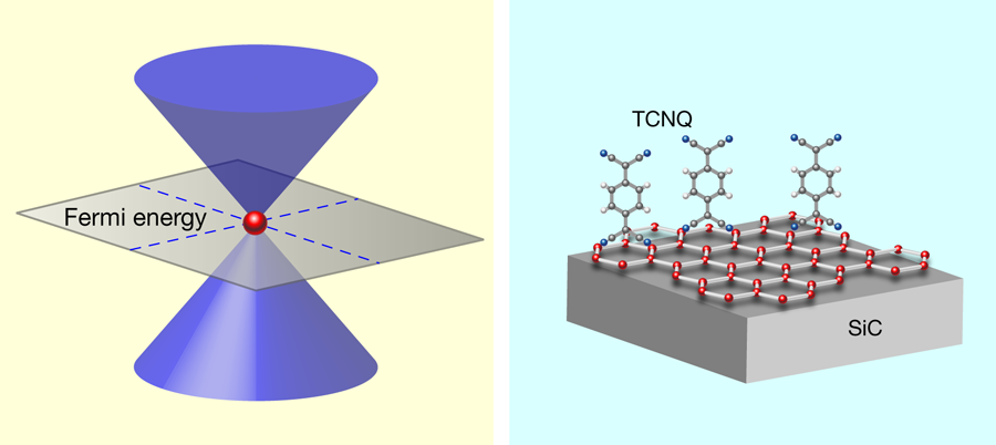
Graphene hardly needs an introduction. This single-atom carbon layer peeled from a piece of bulk graphite possesses many remarkable properties that have, promptly, since graphene’s discovery, been described in excellent reviews [2,3]. Graphene’s peculiar electronic structure—the electron energy depends linearly on momentum, meaning the electrons behave as though they have zero effective mass (Fig. 1, left)—and properties propels it to the front rows of materials being considered for future nanoelectronics devices. Even at room temperature, the mobility of the charge carriers is extraordinarily high (more than 10 times that of comparable semiconductors) and essentially unperturbed by chemical doping.
But, as is usually the case, such an excellent material tends to be in short supply. Making free-standing graphene sheets by exfoliating them from bulk graphite is literally a work of art that, at most, yields samples a millimeter in size. Fortunately, large areas of graphene can be grown on various substrates, and from a technological standpoint, silicon carbide ( SiC) is one of the most attractive options. Large-area samples can be produced in great numbers by simply annealing SiC wafers at high temperature [4]. As one might expect, such simplicity does not come without a sacrifice: the strong interaction between graphene and the SiC substrate leaves the graphene “intrinsically” electron doped and drives the intersection of the occupied and unoccupied states (the “Dirac point”), some 300meV below the Fermi level [5]. The question arises as to whether it is possible to compensate this doping and bring the Dirac point back to the Fermi level, as it would be for free-standing graphene.
For surface scientists, an atomically thin graphene layer on top of a silicon carbide wafer is a familiar object and they know that its electronic structure should be sensitive to the adsorption of atoms and simple molecules. Several research groups have already explored this route and monitored the evolution of graphene electron bands with photoemission while adsorbing NO2 molecules [6] or atoms of bismuth and gold [7].
Experiments with NO2 proved the feasibility of this approach. Depending on the concentration of molecules stuck to the surface, the Fermi level moved all the way to the Dirac point and even crossed it. Moreover, at the stage of the doping where the Dirac point coincided with the Fermi level, graphene became an insulator and photoemission revealed an excitation gap at the Fermi level. (The gap is between two Dirac cones and opens up due to the interaction between graphene and the SiC, which breaks the symmetry of the graphene lattice [8,9].)
While these experiments demonstrated the principle of chemical doping, they could not really be called a technological breakthrough. NO2 isn’t the most user friendly gas. At room temperature it does not stick to graphene in quantities sufficient to induce a shift of the Dirac point and since NO2 easily desorbs from the surface when it is exposed to light, photoemission experiments have to be performed under constant gas flow.
Adsorbing graphene with bismuth, antimony, and gold [7] leads to a similar shift of the Dirac point. Bismuth and antimony, however, do not pin the Dirac point exactly at the Fermi level; rather, it remains about 150meV below it. Gold, on the other hand, induces the shift to approximately 100meV above the Fermi level after the sample is annealed at around 700 ° C.
What is attractive about these approaches is their technological simplicity. Deposition and postannealing are common practices in the semiconductor industry. However, while further work might find a precise correlation between the desired amount of doping and the concentration of atoms and their arrangement on the surface, photoemission data reveal a drawback of doping with gold. The 1s core level of carbon is split, suggesting that graphene and gold form a chemical bond, which could in turn disrupt graphene’s band structure. It is also possible that upon annealing, gold migrates below the graphene layer.
In pursuit of a technologically feasible material, Coletti et al. [1] turned their attention to tetrafluoro-tetracyanoquinodimethane (F4-TCNQ), a compound with a successful track record as an electron acceptor in organic light emitting diodes [10]. Earlier experiments and calculations gave a hint that F4-TCNQ dopes grahene with holes [11,12]. Employing the most advanced ARPES instrumentation, Coletti et al. performed a careful study of graphene with F4-TCNQ deposited on its surface. The group proved that a film of F4-TCNQ with a nominal thickness of 0.8nm, which corresponds to a complete dense layer of molecules, nicely compensates intrinsic electron doping of the graphene layer grown on SiC (Fig. 1, right); namely, the Dirac cone has its tip exactly at the Fermi level and the graphene sample is charge-neutral. As expected, since charge transfer occurs at the interface between F4-TCNQ and graphene, increasing the thickness of the organic complex beyond the first layer does not produce more holes in graphene or affect its band structure.
The organic films are fairly stable. The position of the Dirac cone did not change when the sample was heated up to about 75 ° C and prolonged exposure to light did not harm the organic films either. Perhaps the most stimulating result is that the doping works when F4-TCNQ is applied via wet chemistry (as opposed to vapor deposition in a vacuum chamber). Although this may seem like a detail of the experimental method, in fact the ability to deposit F4-TCNQ from solution means it will, in principle, be possible to take a prefabricated, complex nano-object made from graphene and alter its electronic structure.
Coletti et al.’s recipe for hole-doping graphene may well have an impact on another set of materials. Dirac cones, like those in graphene (Fig. 1, left) are the hallmarks of a class of materials called “topological insulators,” where they exist at the surfaces of bulk insulators, such as Bi2Se3 and Bi2Te3 . There is a great desire to control the surface electronic structure in topological insulators via chemical doping. As one study has already achieved this by adsorbing NO2 molecules on the surface of Bi2Se3 [13], it is possible that Coletti et al.’s work will provide an easy and effective alternative.
References
- C. Coletti, C. Riedl, D. S. Lee, B. Krauss, L. Patthey, K. von Klitzing, J. H. Smet, and U. Starke, Phys. Rev. B 81, 235401 (2010)
- A. K. Geim and K. S. Novoselov, Nature Mater. 6, 183 (2007)
- A. K. Geim, Science 324, 1530 (2009)
- I. Forbeaux, J.-M. Themlin, , and J.-M. Debever, Phys. Rev. B 58, 16396 (1998)
- E. Rollings, G.-H. Gweon, S. Y. Zhou, B. S. Mun, J. L. McChesney, B. S. Hussain, A. V. Fedorov, P. N. First, W. A. de Heer, and A. Lanzara, J. Phys. Chem. Solids 67, 2172 (2006)
- S.Y. Zhou, D. A. Siegel, A.V. Fedorov, and A. Lanzara, Phys. Rev. Lett. 101, 086402 (2008)
- I. Gietz, C. Riedl, U. Starke, C. R. Ast, and K. Kern, Nano Lett. 8, 4603 (2008)
- S. Y. Zhou, G.-H. Gweon, A. V. Fedorov, P. N. First, W. A. de Heer, D.-H. Lee, F. Guinea, A. H. Castro Neto, , and A. Lanzara, Nature Mater. 6, 770 (2007)
- S. Kim, J. Ihm, H. J. Choi, and Y-W. Son, Phys. Rev. Lett. 100, 176802 (2008)
- J. Guo, N. Koch, S. L. Bernasek, and J. Schwartz, Chem. Phys. Lett. 426, 370 (2006)
- W. Chen, S. Chen, D. C. Qi, X. Y. Gao, and A. T. S. Wee, J. Am. Chem. Soc. 129, 10418 (2007)
- H. Pinto, R. Jones, J. P. Goss, and P. R. Briddon, J. Phys. Condens. Matter 21, 402001 (2009)
- D. Hsieh, Y. Xia, D. Qian, L. Wray, J. H. Dil, F. Meier, J. Osterwalder, L. Patthey, J. G. Checkelsky, N. P. Ong, A. V. Fedorov, H. Lin, A. Bansil, D. Grauer, Y. S. Hor, R. J. Cava, and M. Z. Hasan, Nature 460, 1101 (2009)