Graphene prêt-à-porter
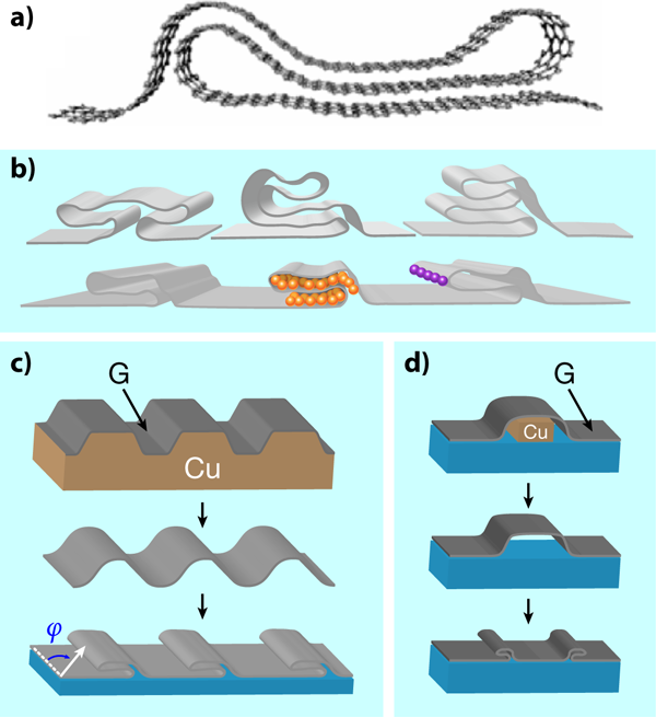
Perhaps the main attribute of graphene is that it is a material of many attributes. It is the thinnest possible membrane, extremely stiff, impermeable, stable, transparent, and one of the best conductors of electricity. Now, through work reported in a paper in Physical Review B, Kwanpyo Kim and collaborators [1] at the University of California at Berkeley and the Lawrence Berkeley National Laboratory have added another item to the list. Like a piece of fabric or plastic wrap, two-dimensional graphene can be manipulated into a third dimension by folding [Fig. 1(a)]. The authors tailor a sheet of graphene into complex shapes they call grafold [Fig. 1(b)]—double or triple folds, hems, ripples, ruffles—taking advantage of its flexibility and mechanical stability. Moreover, they control the orientation, number, and placement of the folded structures. With their technique, new possibilities emerge, like encapsulation of atoms and molecules in the folded regions, chemical functionalization of the reactive folds, interesting electrical, optical, and mechanical properties of periodic folded structures, etc.
One of the key ideas that motivated the experiments leading to the discovery of graphene in 2004 was the search for the thinnest possible metal. Conventional metals become discontinuous when thin, breaking up into small droplets. A different kind of material, one with stronger bonds between its atoms, was needed. However, such chemical structure normally produces insulators. Graphene is an exception: a two-dimensional crystalline macromolecule—with highly packed and strongly bound carbon atoms—that is a conductor, although its transport characteristics differ from those of a typical metal (or a typical semiconductor, for that matter). Moreover, graphene is thermodynamically stable and chemically inert. This means that it can be placed on top of other materials, or be exposed to solvents for cleaning processes, and still preserve its integrity, not merging with its surroundings or getting transformed into a different compound.
Furthermore, graphene is the most reversibly stretchable material ever measured, and may be easily warped in the out-of-plane direction. Not only can it be wrinkled and folded, it is in fact difficult to produce a perfectly flat sheet of graphene. Recently, the flattest graphene layers have been obtained by depositing (or encapsulating) graphene on smooth substrates like boron nitride [2,3] and mica [4]. In general, corrugations appear naturally because graphene adapts to the topography of a rough substrate. Doing away with a substrate does not yield flat graphene; suspended samples spontaneously develop ripples and rolled-up edges. Usually such formations are unwanted and considered as defects. They tend to decrease the high electron mobility and optical transparency of pristine graphene. Random in appearance and arbitrary in shape, they are nontrivial to treat theoretically and end up rendering simple theoretical models of graphene inadequate.
Therefore, the effect of local deformations on graphene is important from a fundamental point of view, as well as technologically relevant. Strains in graphene, for example, have two effects. On the one hand, they modify the electron-hopping amplitudes between neighboring carbon atoms, creating pseudomagnetic fields for the charge carriers. On the other hand, they induce local changes in the density of electrons, giving rise to scalar potentials. Both effects modify quasiparticle transport in a form that is well accounted for by theory [5]. Controlling formation of local strains should enable experimentalists to control electron transport in a reversible manner. This idea gave rise to the concept of strain engineering of graphene’s electronic structure [6]. An extension of the concept is to fold the space in which electrons reside. In the presence of an external and constant magnetic field, for example, the magnetic flux can change sign across the fold, creating an inhomogeneous magnetic landscape for carriers [7,8]. The magnetic flux varies over very short distances (controlled by the fold radius), something more difficult to achieve in conventional semiconductor heterostructures.
Folds and local deformations may prove to be desirable after all. Several ways to create them have already been presented in the literature, although they are produced in a quite uncontrolled way. These include, for example, spontaneous edge reconstruction after heating several layers of graphene [9,10], or free folding under random ultrasonic stimulation of suspended flakes in liquids [11]. Researchers, though, would prefer to control the shape, the position, the orientation, and the number of such modulations. This is precisely what Kim and collaborators achieve in their beautiful work, either by inducing folds during the synthesis or the transfer process of graphene. In the first case [Fig. 1(c)], graphene is grown on a substrate, such as copper, patterned with parallel trenches or similar structures. The folds form during growth, and survive upon transfer to a different isotropic substrate, where they relax. In the second case [Fig. 1(d)], the monolayer is synthesized on an unpatterned substrate, and then transferred to a medium with removable features, such as the copper rail in the figure. These features are then etched away, allowing the slack graphene to collapse, generating a fold in the desired place.
The sophisticated structures the authors produce are very interesting because they present a compendium of several nontrivial aspects: (i) They produce junctions where the number of layers change from one region to another, i.e., a monolayer sheet changes to two, three, or four layers, which then revert to a single layer. Confinement effects arising from the finite size of the multiply folded region are expected. (ii) Strains appear at the edges where the graphene membrane folds. (iii) In multilayer regions, different planes may interact, like in graphite. In such cases, the relative orientation between adjacent layers is crucial, since we know that the precise way atoms of different layers align gives rise to different band structures. The authors carry out first-principles calculations for a system like the one in Fig. 1(a) and find an unconventional band structure that is neither that of graphene (or its bilayer or trilayer version) nor that of a semiconductor. The lowest bands exhibit a semimetallic character with a small, indirect overlap of a few . As the authors claim, this is just one example of the peculiar properties of a system where several effects come into play.
This paper is particularly inspiring for its various prospects. A fascinating possibility is that of a periodic folding structure—a superlattice—in which one can control the width and frequency of the repeated motif. The authors explore one-dimensional arrays but it should also be possible to create two-dimensional periodic structures similar to the one showed in Fig. 1 (c), but with patterned domes in the copper substrate. Yet another interesting advance would be producing the same structures as those reported in the paper but with bilayer graphene, which shares the monolayer’s amazing mechanical stability, and adds the possibility of controlling electrons by applying an interlayer electrostatic bias. One could also try to embed magnetic impurities in the folds, or get rid of the interlayer interaction at desired regions with insulating buffer materials. In a similar vein, it would be interesting to explore multiply folded structures with encapsulated graphene in boron nitride. Would such a sandwich also easily fold and resist strains? Regarding the connection to plasmonics, how could folded structures be employed to enhance and control optical fields? To conclude, the three-dimensional character of grafold structures offers a wide range of possibilities beyond those found in traditional graphene, from the engineering of novel electronic properties to the design of new optoelectronic and mechanical applications.
References
- K. Kim, Z. Lee, B. D. Malone, K. T. Chan, B. Alemán, W. Regan, W. Gannett, M. F. Crommie, M. L. Cohen, and A. Zettl, Phys. Rev. B 83, 245433 (2011)
- C. R. Dean, A. F. Young, I. Meric, C. Lee, L. Wang, S. Sorgenfrei, K. Watanabe, T. Taniguchi, P. Kim, K. L. Shepard, and J. Hone, Nature Nanotech. 5, 722 (2010)
- A. S. Mayorov, R. V. Gorbachev, S. V. Morozov, L. Britnell, R. Jalil, L. A. Ponomarenko, P. Blake, K. S. Novoselov, K. Watanabe, T. Taniguchi, and A. K. Geim, arXiv:1103.4510 (2011)
- C. H. Lui, L. Liu, K. F. Mak, G. W. Flynn, and T. F. Heinz, Nature, 462, 339 (2009)
- A. H. Castro Neto, F. Guinea, N. M. R. Peres, K. S. Novoselov, and A. K. Geim, Rev. Mod. Phys. 81, 109 (2009)
- V. M. Pereira and A. H. Castro Neto, Phys. Rev. Lett. 103, 046801 (2009)
- E. Prada, P. San-Jose, and L. Brey, Phys. Rev. Lett. 105, 106802 (2010)
- D. Rainis, F. Taddei, M. Polini, G. Leon, F. Guinea, and V. I. Falko, Phys. Rev. B 83, 165403 (2011)
- J. Huang, F. Ding, B. Yakobson, P. Lu, L. Qi, and J. Li, Proc. Natl. Acad. Sci. U.S.A. 106, 10103 (2009)
- Z. Liu, K. Suenaga, P. J. F. Harris, and S. Iijima, Phys. Rev. Lett. 102, 015501 (2009)
- J. Zhang, J. Xiao, X. Meng, C. Monroe, Y. Huang, and J.-M. Zuo, Phys. Rev. Lett. 104, 166805 (2010)