A useful pyramid scheme
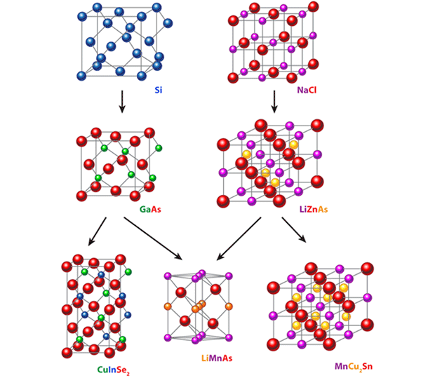
All our electronics technologies have, at their heart, critical materials that make their function possible. These can be “old” materials such as silicon, whose major materials development was achieved by previous generations, or “new” materials such as gallium-nitride, which has been developed by our contemporaries (Fig. 1). The impact of these two materials on society is, and will be, immeasurable, as are the contributions of many other materials in technologies that range from medical imaging to portable electronics. If the discovery and development of new materials comes to a stop, then the introduction and growth of new technologies will almost certainly come to a halt as well. Spintronics is an example of such a critical current technology, driving the creation of increased density, faster electronic memories through the electronic manipulation of magnetic moments. In a paper published in Physical Review B [1], Tomas Jungwirth and collaborators from the Institute of Physics of the Academy of Sciences of the Czech Republic, and collaborators from the Czech Republic and the United Kingdom, report the successful growth and characterization of LiMnAs, a new candidate material for spintronic applications.
But where do new materials come from? How do they go from an idea to an application? This is an important, multifaceted issue to address for individuals and organizations interested in forefront issues in science or the development of new technologies, and on a larger scale, for countries that care to have a robust technological sector. New materials, of course, come from our research and engineering communities. A big-picture treatment of some of the systemic issues and ways that they might be addressed can be found in a recent National Research Council report dealing with exactly this question [2]. Many countries have recognized the need for new materials development and have addressed it in ways consistent with their own culture and socioeconomic system. The systems that seem to completely fail in this regard are those that invest only in the technologies of the here and now, without looking more than a few years ahead.
Most relevant to a discussion of the paper by Jungwirth et al. on the potential of LiMnAs and related compounds for spintronics are the scientific aspects of where new materials come from. From my point of view, a good place to start is the “Sales Materials Pyramid,” a concept developed by Oak Ridge National Laboratory materials scientist Brian Sales, which I will elaborate a little on here. At the base of the materials pyramid are what chemists call “new materials”—these are previously unreported solid compounds that have been found, and chemically and structurally characterized, by solid-state chemists specializing in the new compound discovery process. There are hundreds of such totally new compounds discovered every year. They are virtually always magnetically or electronically characterized in only a cursory fashion, as the chemists are not expert in materials properties, but they form a critical knowledge base for the upper tiers of the pyramid. The next tier is where the materials physicists come into the picture. Having a particular property in mind, they notice a material previously reported by chemists that may display a particularly interesting property. The discovery of an interesting property at this stage results in what is called, fairly enough, a “new material” in materials physics, even if its existence has already been reported in the literature. At this tier, materials physicists will undertake the development of higher quality samples, typically through the growth of small crystals. This tier is smaller than the base, and smaller still is the third tier, where only the most interesting of these new materials are selected for further refinement of the physics—often along with the growth of larger, higher quality crystals and thin films for the testing of new devices—and input from theory. In the next tier, experts in technologies take over the process, selecting only some materials for integrating into their systems when they see that the potential benefit of including a new kind of material outweighs the down side of having to redesign devices or fabrication processes to accommodate it. Obviously, if the technology itself is new, and is enabled by the new material, then the barrier to incorporation of the new material is small. Finally, we have the tip of the pyramid, the even smaller number of materials which, through continuing development, make it into real technologies and benefit society. It can take a long time for a material to proceed from the base to the tip, but the process is worth the investment.
Carefully reading the paper by Jungwirth et al. provides an excellent tutorial on taking a material up the first few tiers in the materials pyramid, an accomplishment that one almost never sees in a single publication. What are the steps that their work illustrates? Step 1: Identify a scientific or technological problem that might be advanced by the application of a new material. Step 2: Study the literature to learn which materials are currently known that do the job fairly well. Identify their shortcomings and come up with an idea about how the shortcomings might be addressed, and identify a candidate in a lower tier of the pyramid that might do it. Step 3: Form a team of researchers whose specialties and interests are complementary, make the material, and test to see whether your idea is right. Include theory to help you to interpret your results. Step 4: Make the new material in the critical physical form needed to determine whether it has any chance of being useful in the device of interest.
Let’s briefly summarize what Jungwirth et al. have done. Step 1—The problem: The continuing development of room-temperature, faster, higher density electronic devices that can be easily integrated into microelectronics technologies is obviously beneficial to society. The current generation of “spintronics” devices, based on metallic ferromagnets, works very well (see, e.g., Ref. [3]) but is fundamentally limited by the fact that the enabling materials are metals. Can some of these limitations be overcome by designing devices that employ processing-compatible insulating or semiconducting ferromagnetic or antiferromagnetic materials whose spins can be manipulated by microelectronics accessible voltages? Step 2—Develop a candidate material: The authors have done a substantial service to the community by describing the process they used, which is a combination of looking at what chemists would call “derivative structures,” chemical-structural compatibility, and physics-based arguments for what the critical electronic characteristics of the material should be. Through this process they arrive at the selection of an obscure material, LiMnAs, studied in the 80s, but never graduating above the first tier of the pyramid. The use of derivative structures is a particularly important concept in discovering new materials and is highlighted in Fig. 1. The authors have tested LiMnAs, likely at an early stage in the process, by performing electronic structure calculations to confirm that it is intrinsically semiconducting, and to confirm that the previously observed antiferromagnetism makes sense within current theoretical models for the descriptions of magnetic materials. Step 3—Test the idea: Is the idea a good one? Does it work? To answer these questions the authors had to combine Steps 3 and 4. They successfully fabricated good quality epitaxial films of the candidate compound on an InAs substrate, proving that it can indeed be made in the form needed for potential device applications and also demonstrating its compatibility with a well-established semiconductor materials system. This is a big step for a new material and certainly must have represented a significant scientific, and even psychological, challenge, since putting an alkali metal (i.e., Li) into an Molecular Beam Epitaxy apparatus sounds like something that very few of the owners of such instruments would dare try (because Li vapor might be expected to attack the machine’s guts, or at least hang around in there forever).
The authors have shown convincing evidence of epitaxy and good film quality, and shown that LiMnAs is a semiconductor by performing optical spectroscopy, and also that it is antiferromagnetic in thin film form (consistent with earlier reports on the bulk material) by measuring its temperature-dependent magnetization. Performing all these steps required a large team of people; 17 coauthors is an unusually large collaborative group in materials physics. Thus they have taken a material from tier 1 to tier 4 in a single paper. Now it is ready for others, maybe even these researchers, to take to the next tier. Will this particular material go further? It is hard to tell at this stage, as the mobility of Li may turn out to be a show stopper (destabilizing device structures), but the work does provide an inspiration for thinking about other materials that could also do the trick.
Spintronics is a very rapidly developing field, and the group that has written this paper, along with others equally innovative, is making significant contributions to its advancement. Given the substantial benefits that fast, high-density memories would have to society, and the fascinating, complex materials chemistry, materials physics, and electronics engineering problems that researchers in this field have to solve to advance, it seems like an excellent area in which to work. The paper by Jungwirth et al. and the references therein provide an excellent entry point for people looking to learn about it. One gets the distinct impression that revolutionary changes are in the near future, and that some of the new materials proposed that enable novel kinds of devices will make it to the tip of the Sales pyramid in a relatively short time.
References
- T. Jungwirth et al., Phys. Rev. B 83, 035321 (2011)
- Frontiers in Crystalline Matter: From Discovery to Technology, National Research Council (National Academies Press, Washington DC, 2009)[Amazon][WorldCat]
- Albert Fert, Rev. Mod. Phys. 80, 1517 (2007)