Nanoparticles in Hiding
The design of artificial metamaterials that allow “cloaking”—apparent invisibility to acoustic and electromagnetic waves—is more than a party trick. Many applications suggest themselves if one could create cloaking at useful frequencies or in technologically relevant systems. Writing in Physical Review Letters, Bolin Liao and colleagues at Massachusetts Institute of Technology, Cambridge, propose the use of cloaking in semiconductor devices to optimize electron mobility in nanostructured materials.
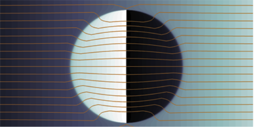
As semiconductor devices are miniaturized to smaller and smaller sizes, having proper control over electron scattering and transport becomes more and more significant. Could one create scattering centers in a semiconductor that are transparent at certain energies? The team presents a description of core-shell nanoparticles in a semiconductor matrix host where the nanoparticles are of a similar size to the electron wavelength. The nanoparticles would then be invisible to electrons, improving the electron mobility at these energies, with associated tunability.
As an analogy to the Mie theory for electromagnetic scattering problems, the partial-wave formalism expresses the total scattering cross section as a summation of contributions from “partial waves” with different angular momenta. To be practical, the nanoparticles would be of a similar size to the electron wavelength; thus higher order partial waves would inevitably contribute. Working under this framework, they adjust the electron wavelengths, the core-shell ratio, and the effective mass of the core and shell materials to achieve four orders of magnitude decrease in scattering within a narrow energy range. Liao et al. suggest an implementation that involves a gallium arsenide two-dimensional system, as well as a three-dimensional scheme involving thermoelectric materials. Possible applications of these “electron cloaks” include novel electronic switches and sensors, and efficient energy harvesting and conversion techniques. – Daniel Ucko