Holes in Silicon Hold On to Their Spin
In spintronic devices [1–3], digital information is represented by the direction of the quantum-mechanical spin of the charge carriers. A spin pointing in one direction denotes a logical , whereas a spin pointing in the opposite direction represents the logical . Spintronic devices are almost exclusively fabricated out of -type semiconductors (electrons carry the current) as opposed to -type semiconductors (holes carry the current), which may seem surprising since both electrons and holes have spin. The reason is that holes have been assumed to be unable to preserve their spin polarization over distances longer than a few tens of nanometers. This perspective is changing, as several recent experiments have shown that hole spins in -type silicon can be polarized and retain their polarization for a surprisingly long time. However, experiments that directly probe the spin of the holes as they travel through the material have been lacking.
Eiji Shikoh at Osaka University, Japan, and colleagues have now performed such an experiment [4]. Writing in Physical Review Letters, Shikoh et al. use a new approach to show that holes in -type silicon can preserve spin-based information and transport it over distances much longer than previously thought. Taken together, the new work and the previous experiments support the view that spin transport is realistic in -type semiconductors. This opens the door to developing spintronic devices and circuits that exploit the unique features of -type semiconductors and their combination with -type materials.
One of the challenges for spintronics is that semiconductors are not ferromagnetic: in equilibrium, the spins randomly point in all directions. In order to study the behavior of spins in semiconductors and exploit them to perform computations, one has to give a population of spins a preferred orientation such that its average is nonzero. But as soon as the source of spin generation is turned off, the spin polarization decays back to zero. The decay is typically exponential and the associated time constant is referred to as the spin-relaxation time, the value of which is an important parameter for spintronic devices and systems. The spin-relaxation time determines how long a nonequilibrium spin polarization can persist, and thereby, how far carriers can travel (by diffusion or drift) before the spin orientation randomizes and spin information is lost.
Conduction electrons in silicon and gallium arsenide, two of the most widely used semiconductors, have a spin-relaxation time between one and a few hundred nanoseconds. (The actual value depends on the temperature and doping density of the semiconductor.) For doped -type silicon, the spin-relaxation time is a few nanoseconds at room temperature—long enough that conduction electrons can preserve their spin orientation over a distance of a micrometer or so. The relatively large spin lifetime for electrons is a consequence of the weak spin-orbit interaction between a charge’s spin and its orbital angular momentum in the silicon conduction band. As a result, the states are well described with a unique spin angular momentum ( or , with equal to Planck’s constant divided by ). Moreover, the local spin-orbit interaction associated with typical dopant impurities is also weak. Therefore, even if the electron is scattered by dopant impurities, the electron’s spin remains relatively unaffected.
The situation is quite different for the spins associated with mobile holes. Unlike electrons in the conduction band, holes in the valence band are more strongly affected by the spin-orbit interaction because the valence band is derived from states with a nonzero orbital momentum. As a result, hole states can’t be described with a definite spin or , but rather a mixture of the two. A change of the spin is then expected whenever the hole is scattered and a state with a different spin mixture is obtained. The spin lifetime is therefore expected to be of the order of the scattering time of the conduction holes, which is well below a picosecond (ps) and very short indeed.
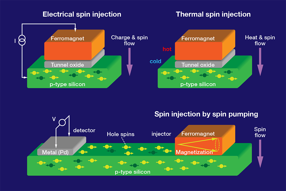
Recent advances [3] in the creation and electrical detection of spin polarization in semiconductors have made detailed studies of hole spin polarization possible, and challenged the view that the relaxation time of spins in -type materials is very short. In 2009, it was demonstrated that a spin polarization can be created and detected at room temperature, not only in -type silicon, but, unexpectedly, also in -type silicon [5]. In these experiments, the source of the spins was a ferromagnet (Fig. 1, top left): a spin-polarized charge current was sent from the ferromagnet into the silicon by tunneling, producing an injection of spins with a preferred orientation. The hole spin lifetime extracted from those experiments was a few hundred picoseconds. Subsequently, it was shown that a charge current wasn’t even necessary for spin transport: a heat flow across a magnetic tunnel contact could also induce a spin polarization in -type silicon (Fig. 1, top right) [6].
More recently, the technique of spin pumping [7] has been used to successfully inject spin-polarized holes from a transparent ferromagnetic contact into -type silicon [8]. In this technique, a microwave magnetic field induces resonant rotation of the magnetization of the ferromagnet. The magnetization dynamics is accompanied by a spin current that is pumped across the ferromagnet-semiconductor boundary.
Shikoh et al. [4] have taken a different approach, compared to previous experiments [5,6], in that they separated the process of spin injection and detection. This allowed them to probe the spin of the holes after travelling through the material. In their measurement device, Shikoh et al. used the spin-pumping method to inject spins into their silicon sample, and did not apply an electric field, so the injected spins spread out under the injection contact by spin diffusion (spin diffusion is driven by the gradient in the spin density). They placed their spin polarization detector—a contact made out of a nonmagnetic metal that absorbs part of the spin current and converts it into a transverse charge voltage—a few hundred nanometers (nm) from the point of injection (Fig. 1, bottom).
What Shikoh et al. [4] have convincingly demonstrated is that a spin current injected into their -type silicon device is able to traverse the more than nm to the palladium detector contact, arriving with its spin polarization mostly preserved. Clearly, this would not be possible if the spin lifetime of holes was only a fraction of a picosecond: the corresponding spin-diffusion length would have been only nm or so—a tiny fraction of the device’s size. In fact, the authors extract a spin-diffusion length of about nm and a spin lifetime of about ps for holes in silicon at room temperature. These values are close to those obtained by Dash et al. [5].
Shikoh et al. have presented a powerful and complementary method to probe the behavior of hole spins. One obvious extension is to study the (exponential) decay of the spin signal as a function of the distance between the injector and detector contact. This would allow a more direct determination of the spin-diffusion length. Perhaps more importantly, with the new results by Shikoh et al. there now exists a significant body of work based on different approaches that all point in the same direction: the spin lifetime for holes in -type silicon is much larger than previously thought. A similar picture is beginning to emerge for the spins associated with holes in -type germanium [3,9]. In contrast, the hole spin lifetime in -type gallium arsenide seems to follow the established view, as it was found to be of the order of a few hundred femtoseconds [10]. It remains an open challenge to figure out why spin transport in some -type semiconductors behaves as expected and in others it does not: we simply don’t know the answer to this puzzle yet. In any case, -type silicon is now established as a carrier of spin information and can be added to the toolkit of materials for spintronics.
Correction (19 March 2013): Reference 6, volume 471 changed to 475.
References
- C. Chappert, A. Fert, and F. Nguyen van Dau, “The Emergence of Spin Electronics in Data Storage,” Nature Mater. 6, 813 (2007)
- A. Fert, “Nobel Lecture: Origin, Development, and Future of Spintronics,” Rev. Mod. Phys. 80, 1517 (2008)
- R. Jansen, “Silicon Spintronics,” Nature Mater. 11, 400 (2012)
- E. Shikoh, K. Ando, K. Kubo, E. Saitoh, T. Shinjo, and M. Shiraishi, “Spin-Pump-Induced Spin Transport in p-Type Si at Room Temperature,” Phys. Rev. Lett. 110, 127201 (2013)
- S. P. Dash, S. Sharma, R. S. Patel, M. P. de Jong, and R. Jansen, “Electrical Creation of Spin Polarization in Silicon at Room Temperature,” Nature 462, 491 (2009)
- J. C. Le Breton, S. Sharma, H. Saito, S. Yuasa, and R. Jansen, “Thermal Spin Current from a Ferromagnet to Silicon by Seebeck Spin Tunneling,” Nature 475, 82 (2011)
- A. Brataas, G. E. W. Bauer, and P. J. Kelly, “Non-collinear Magnetoelectronics,” Physics Rep. 427, 157 (2006)
- K. Ando and E. Saitoh, “Observation of the Inverse Spin Hall Effect in Silicon,” Nature Commun. 3, 629 (2012)
- S. Iba, H. Saito, A. Spiesser, S. Watanabe, R. Jansen, S. Yuasa, and K. Ando, “Spin Accumulation in Nondegenerate and Heavily Doped -Type Germanium,” Appl. Phys. Express. 5, 023003 (2012)
- D. J. Hilton and C. L. Tang, “Optical Orientation and Femtosecond Relaxation of Spin-Polarized Holes in GaAs,” Phys. Rev. Lett. 89, 146601 (2002)