Landmarks—The Birth of Photonic Crystals
Landmarks articles feature important papers from the archives of the Physical Review journals.
Photonic crystals, structures that allow researchers to manipulate the passage of electromagnetic radiation, went from theoretical possibility to experimental reality over a period of several years. Two papers in Physical Review Letters, in 1987 and 1991, stand as bookends to the emergence of these new structures. Since then, researchers have used photonic materials to guide light in devices such as fiber optics and have also realized that such materials exist in nature, for example in the scales that give butterfly wings their iridescent colors.
In the 1980s, Eli Yablonovitch, then at Bell Communications Research (now part of Ericsson) in Red Bank, New Jersey, was worried about losses in semiconductor lasers and other devices arising from light emitted at unwanted frequencies. In a 1987 paper in Physical Review Letters he observed that these losses would not occur in a medium that prevented these frequencies of light from propagating. He proposed that such a medium could be made by carving out voids in a transparent material to create a periodic structure, analogous to a crystal lattice, with the material and the voids having different indices of refraction (different speeds of light).
Yablonovitch offered an analogy to semiconductors, which have an energy “band gap” between the valence electrons—associated with chemical bonds—and the conduction electrons. Just as electrons with energies in the band gap cannot exist in a semiconductor, so light with frequencies in the electromagnetic band gap would not exist in the proposed structure. In each case, the periodic structure leads to destructive wave interference (electron waves or electromagnetic fields) that leads to the gap.
It happened that Sajeev John of Princeton University independently made a related proposal at the same time [1]. Yablonovitch, now at the University of California, Berkeley, says that he and John met to discuss their ideas and decided to use the words “photonic crystal” to describe structures with band gaps for electromagnetic waves.
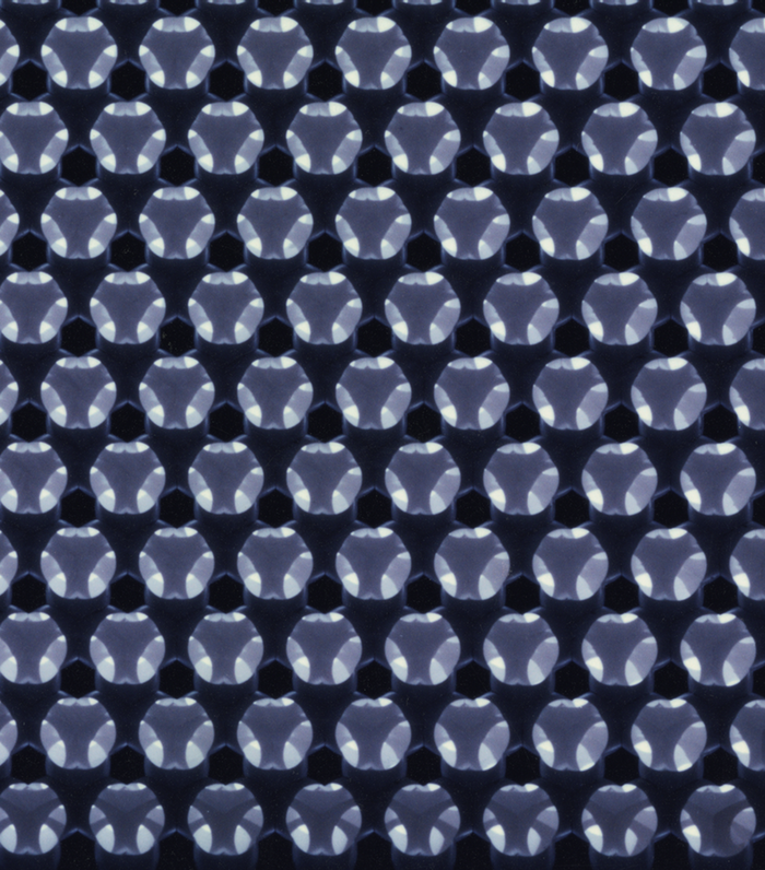
In trying to make a photonic crystal, Yablonovitch worked with microwaves, rather than visible or infrared light, because their longer wavelengths allowed him to develop periodic designs with spacings on the scale of a few millimeters. In 1989, after testing many different possibilities, he and T. J. Gmitter published what they claimed to be the first structure with a photonic band gap, consisting of spherical holes arrayed throughout a block of plastic in a face-centered cubic (fcc) pattern [2]. Both Yablonovitch and John favored such structures, thinking that because the fcc pattern is close to isotropic, it ought to block radiation in all directions, and the measurements seemed to agree.
Spurred by this paper, theorists worked out how to apply Maxwell’s equations to photonic structures. However, three analyses of the Yablonovitch-Gmitter structure indicated that it had only a “pseudogap,” meaning that the forbidden frequency range shrank to zero for certain directions of radiation [3,4]. That was a shock, says Yablonovitch, but he realized that his measurements had not been comprehensive enough.
Building a structure with an omni-directional band gap took another two years. In their 1991 paper, Yablonovitch and Gmitter were joined by one of the theorists who had criticized their earlier work, K. Ming Leung of Polytechnic University (now Polytechnic Institute of New York University). The team described a structure that, according to both experiment and theory, possessed a true photonic band gap—one that prevented radiation in all directions.
To create the structure, the team drilled a series of holes through a solid block of plastic. Starting with a triangular array of target points on the top surface, they drilled three holes at each point, each time angling the bit at 35° from vertical but rotating horizontally to get three equally-spaced directions as seen from above. The pattern turned out to be a variety of fcc related to the crystal structure of diamond, which was suggested by one of the earlier theoretical analyses to possess a true band gap [4]. The team got the widest band gap when the hole diameter was so large that the drilled-out volume amounted to 78% of the total structure.
Although it was several more years before the first photonic crystal for optical wavelengths was made [5], Yablonovitch regards his 1987 paper as the beginning of photonic crystals. John Joannopoulos of the Massachusetts Institute of Technology agrees that the paper was important for “throwing out an idea,” although it offered no proof of the concept. Ironically, he says, it was the erroneous 1989 structure that got more attention and caused the theorists to jump in, which led to the first true photonic band gap. In recent years, photonic crystals have been used for several purposes, such as optical fibers that in some cases confine light more effectively than traditional fibers (more examples in technology and nature).
–David Lindley
David Lindley is a freelance science writer, now retired. His most recent book is The Dream Universe: How Fundamental Physics Lost Its Way (Penguin Random House, 2020).
References
- S. John, “Strong Localization of Photons in Certain Disordered Dielectric Superlattices,” Phys. Rev. Lett. 58, 2486 (1987)
- E. Yablonovitch and T. J. Gmitter, “Photonic Band Structure: The Face-Centered-Cubic Case,” Phys. Rev. Lett. 63, 1950 (1989)
- K. M. Leung and Y. F. Liu, “Full Vector Wave Calculation of Photonic Band Structures in Face-Centered-Cubic Dielectric Media,” Phys. Rev. Lett. 65, 2646 (1990); Z. Zhang and S. Satpathy, “Electromagnetic Wave Propagation in Periodic Structures: Bloch Wave Solution of Maxwell’s Equations,” Phys. Rev. Lett. 65, 2650 (1990)
- K. M. Ho, C. T. Chan, and C. M. Soukoulis, “Existence of a Photonic Gap in Periodic Dielectric Structures,” Phys. Rev. Lett. 65, 3152 (1990)
- S. Y. Lin, J. G. Fleming, D. L. Hetherington, B. K. Smith, R. Biswas, K. M. Ho, M. M. Sigalas, W. Zubrzycki, S. R. Kurtz, and Jim Bur, “A Three-Dimensional Photonic Crystal Operating at Infrared Wavelengths,” Nature 394, 251 (1998)
More Information
Examples of photonic crystals in commercial technology and in nature (E. Yablonovitch, Univ. of California, Berkeley)