Atom-Scale Ohmmeter
A scanning tunneling microscope (STM) can make an image of individual atoms on a surface or move single atoms around. Now researchers have pushed the device’s precision and used it to measure the differences in electrical conductance between different locations around a single atom on a lead surface. The results could help elucidate the properties of metals and superconductors and might one day find use in nanotechnology fabrication.
An STM brings a needle-like probe—the tip of which is a single atom—extremely close to a sample surface in a vacuum. When voltage is applied, electrons can jump, or “tunnel,” across the gap, and measuring the resulting current while moving the tip across the surface leads to an image. In another STM technique, the probe tip touches the sample, allowing atoms to chemically bond with it. Researchers have used this method, known as point contact, to move atoms around like toy blocks. The point contact technique would also be appropriate for measuring electrical conductance of a material at the atomic scale, to learn how current flows in the quantum regime, where the classical Ohm’s law fails.
The problem is that when the tip touches the surface, it may rearrange or damage the sample, or even drop nanometer-sized chunks onto it. These effects make it impossible to maintain the consistent tip and surface needed to image a region of atoms and keep track of the tip’s location with the necessary accuracy. Now Yukio Hasegawa and Howon Kim of the University of Tokyo have managed to avoid this so-called “tip crash” by reducing mechanical vibrations and electronic noise and by using an extremely stable tip made of lead. This system allowed the team to directly measure the electrical conductance of lead at precise locations in the atomic structure.
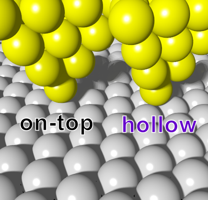
The atoms in a lead lattice are like a field of cannonballs stacked in layers, creating a regular geometric landscape. When the STM tip hovers above this field, and the electrons flow by tunneling, the conductance is relatively uniform. The researchers found that when they brought the tip very close atop an atom, they measured a higher conductance compared with sites between atoms.
But when they allowed the tip to touch the lattice, conductance was greatest in the spaces between atoms, with further differences among the different types of sites. For example, holes where three atoms meet, with an additional atom in the layer below, had the highest conductance, whereas troughs between two side-by-side atoms had an intermediate value.
Based on theoretical modeling, the researchers think the explanation lies in the chemical bonds among the atoms, which provide channels through which electrons can flow. When the STM tip is slightly above but not quite touching the lead lattice, it interacts mostly with an atom sticking up above the field, and so the conductance becomes higher there. But when the probe contacts the metal, it chemically bonds with greater numbers of atoms. The more bonds it forms, the more routes for electrons, and thus, the higher the conductance.
In the future, Hasegawa and Kim hope to use their STM technique to investigate the paired electrons (Cooper pairs) that appear when lead is cold enough to become a superconductor. The team wants to observe the flow of Cooper pairs in the lead lattice, which should similarly depend on the number of available channels. They also think their results could prove useful in the construction of nanoscale devices, where a detailed understanding of electrical flows through different parts of atoms will be crucial.
“What’s nice here is a systematic study,” says STM expert Laurent Limot of the French National Center for Scientific Research (CNRS) at the University of Strasbourg. “They really investigated point by point on the image.” While other teams have made site-specific measurements using different techniques—such as ones that distinguished between single and double bonds in a (buckyball) molecule—Limot says that no one has measured at so many locations with the point contact technique.
This research is published in Physical Review Letters.
–Adam Mann
Adam Mann is a freelance science writer in Oakland, California.