Chip-Size Beam Splitter for Electrons
Most electron beam splitters follow a simple 1950s design in which a charged filament divides the path of a beam of electrons. Researchers have now developed an alternative beam splitting technique that uses electric potentials generated above an electronic chip. With further development, this beam splitter could enable electron interferometry and other quantum optics experiments to be performed on a single chip.
Electron beam splitters currently find use in so-called electron holography, in which microscopic images are produced with the help of interfering electron beams. This technique can be less damaging to a sample than regular electron microscopy when low-energy electrons ( to electron volts) are used for the imaging. However, certain experiments require electron beams with even lower energy and/or a different splitting mechanism that disturbs the electrons less.
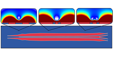
Jakob Hammer and his colleagues at Friedrich-Alexander-University in Erlangen, Germany, have designed a new beam splitter that provides a new range of capabilities. The device would complement recent developments in making chip-based electron waveguides, in which electrons are guided with microwaves generated by long, thin electrodes on the chip surface. For the beam splitter, the electrodes are arranged such that the waveguide splits, or “forks,” into two waveguides. Using an electron gun (like those from old TV sets), the researchers fired electrons with around electron volt of energy into one side of the guide and recorded a double beam coming out the other side, as expected. With modeling, the researchers showed how the splitting can be made smoother (more adiabatic), allowing the two exiting beams to remain more coherent with each other. This could allow for a quantum electron microscope, in which highly fragile biomolecules are placed in one arm of an electron interferometer and are imaged without ever interacting with an electron.
This research is published in Physical Review Letters.
–Michael Schirber


