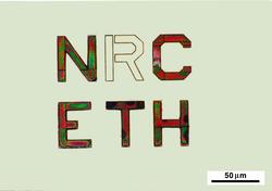
Microscopic Graffiti
Silicon, the raw material of the microchip revolution, can glow at room temperature. Researchers have extensively studied porous silicon–the form of silicon that lights up–in the past decade, because it could lead to electronic circuits seamlessly integrated with fiberoptic cables, displays, and other “optoelectronic” applications. Fundamental questions remain about the material, including the electrochemical process that creates it. In the 4 May PRL, a team dramatically demonstrates a key element of the pore-formation process and exploits it for a new method of precisely “writing” microscopic patterns that can emit light.
Porous silicon is made by submerging a silicon crystal in an acid solution and applying current. An electrochemical process “etches” the surface, creating sub-micrometer-sized pores and crystallites as small as a few nanometers. Just as the spacing between allowed energies of an electron in a box increases with smaller box sizes, the confinement of electron-hole pairs to the silicon crystallites boosts the spacing of their energy levels. Transitions that emit infrared photons in normal silicon, emit in the visible range in porous silicon, and the wavelengths of emission can be tuned by varying the sizes of the crystallites.
To learn more about the pore formation process, David Lockwood and Lynden Erickson, of the National Research Council of Canada in Ottawa (NRC), and Patrik Schmuki, of the Swiss Federal Institute of Technology (ETH), created precisely controlled defects in silicon crystals. They buried extra silicon atoms along narrow paths using a 100-nm-wide beam of Si++ ions to bombard the surface. They could trigger the electrochemical etching process on the “implanted” parts of the surface with a small applied voltage, while the adjacent virgin silicon remained undisturbed, only becoming etched at higher voltages. The results suggest that the pore formation process begins at crystalline defects, rather than at impurities, as some have suggested. At the same time, the team showed how to make microscopic light-emitting patterns of arbitrary shape in silicon, which could be used for the pixels of an all-silicon display, or on-chip light-emitting diodes (LED’s) to couple between chips or into optical fibers.
“It’s a clever technique,” says Philippe Fauchet of the University of Rochester, in New York. He is most impressed by the team’s ability to make sharp boundaries: “They can actually have either etching or no etching,” which he says is “rather important,” compared with other techniques that only influence the degree of etching. According to Fauchet, chip “real estate” is quite valuable, and if manufactures are ever to integrate electronics with porous silicon LED’s, for example, they will want very small light-emitting elements whose construction (etching in acid) will not endanger nearby conventional circuit elements.


