Dark Physics Beats Light Limit
Current laser-based techniques to make computer chips cannot fashion components much smaller than the light’s wavelength, but researchers are devising tricks to beat this so-called diffraction limit. A new idea, detailed in the 22 February Physical Review Letters, is to use a dark state–which requires multiple laser beams–to write patterns in the absorbing material. Calculations show that the technique could create structures far smaller than the beams’ wavelengths without using the dangerously high intensities needed with other proposed techniques.
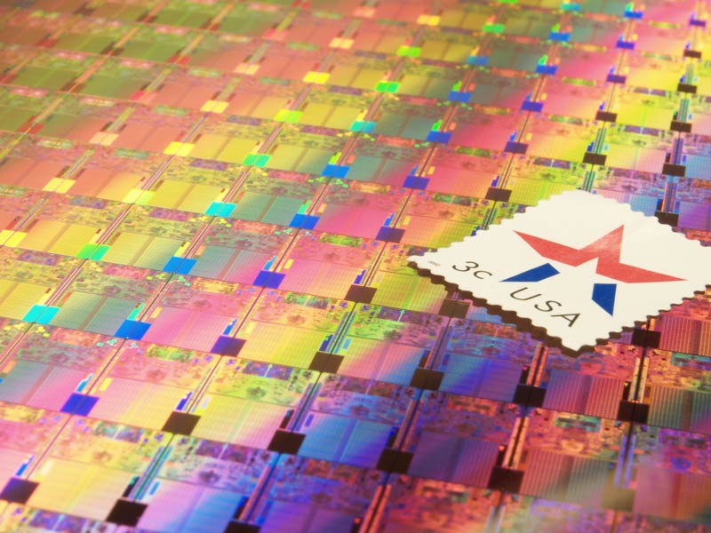
In optical lithography, a “picture” of a microchip circuit is shone onto a semiconductor coated with a light-sensitive material called photoresist. Light-exposed areas of commonly-used photoresists become susceptible to the chemicals that etch out the integrated circuit pattern. According to classical physics, these exposed areas cannot be smaller than half a wavelength of the laser light. Engineers have ways to fudge this limit, such as immersing the semiconductors in liquids that help bend the light further. But to fundamentally break the limit, theorists have proposed systems where the photoresist molecule is activated by two or more photons of light, rather than one. Increasing the excitation energy reduces the effective wavelength, compared with a single photon. But multiphoton absorption requires all of the photons to be in the same place at the same time, which means high laser intensities that could damage materials or equipment.
Now Suhail Zubairy of Texas A&M University’s campus in Qatar and his colleagues from the Max Planck Institute for Nuclear Physics in Heidelberg, Germany, have proposed a new way to get below the diffraction limit without high-intensity lasers. The photoresist molecules would be activated by coherent population trapping (CPT), a process used in slow light and other atomic experiments. In the simplest case, two lasers drive two transitions from different lower energy states to a common excited state, but due to a quantum interference effect, the molecules are never excited. Instead they evolve into a so-called dark state–a stable combination of the lower states that is unaffected by light. With additional upper and lower states, there may exist more complex dark states that combine several low-energy states and that could be populated using additional lasers tuned to the different transitions. CPT does not require multiphoton absorption, so it can work at relatively low intensities.
Zubairy’s team showed that one can use the lasers to create sub-wavelength-sized regions on the surface where the molecules are all in a special state–not simply the dark state, but the dark state “favoring” one of its component low-energy states over the others. In the simplest case, each of the two beams would be split in half and reflected back onto itself to form a pattern of light and dark stripes on the photoresist surface. By arranging how these patterns overlapped, some places would be exposed to more of one laser than the other. The researchers calculated how this varying illumination would affect the molecules in the dark state and found that they formed a pattern of their own–stripes alternating between molecules favoring one of the two component states and those favoring the other.
Assuming one state was more susceptible to etching, the process could lead to chip features as narrow as a half wavelength, according to their calculations. To beat the diffraction limit, the team included a third component in the dark state and an additional pair of lasers in their theory, which reduced the etch-sensitive stripes to quarter-wavelength thickness. More complex dark states led to even narrower stripes. By combining stripes of different widths, engineers could make the complicated patterns for a microchip, say the authors.
Jonathan Dowling of Louisiana State University in Baton Rouge thinks this new idea in “quantum trickery” could work, but the required energy level structure may be hard to reproduce in a commercial photoresist. “A lot of chemistry will be needed to translate these ideas into a practical technology,” he says.
–Michael Schirber
Michael Schirber is a Corresponding Editor for Physics Magazine based in Lyon, France.


