Guiding Surface Waves

Future microchips might manipulate light signals as easily as computer chips handle electronic data–only faster. That dream seems possible using photonic crystals–nanoscale periodic structures that can precisely control light propagation at specific wavelengths. In the 2 April PRL a team shows that another type of light-speed signal called a surface plasmon polariton (SPP) can be manipulated using the same principles. The researchers guided these electron waves along a gold surface with structures that are much easier to make than conventional photonic crystals. The new structures may also lead to new experiments aimed at better understanding SPPs, waves that consist of an unusual interaction between metallic electrons and light.
The key to this type of wave manipulation is the so-called photonic band gap effect. Just as electrons in a silicon crystal cannot exist in the range of energies known as the band gap, light waves in a photonic crystal are forbidden from a specific range of wavelengths. It’s a wave interference phenomenon based on the combined effect of the array of scatterers (atoms in silicon, or reflective zones in photonic crystals). Clear out the scatterers along a narrow path through the photonic crystal, and you have a waveguide–essentially a “wire” for light. Light of the right wavelength is forbidden from venturing off the charted course. Guided this way, light can round a 90-degree turn without losing energy, and researchers hope to connect switches and even microlasers to integrate into “light circuits.”
There have been some technical problems developing photonic crystals, so Sergey Bozhevolnyi of Aalborg University in Denmark and his colleagues wanted to explore an alternative technology based on SPPs. SPPs are waves that result from an intimate interaction between electromagnetic waves and metallic surface electrons. They can’t travel more than a few hundred micrometers before dying out, but for the super-miniaturized integrated circuits he has in mind, Bozhevolnyi says that distance is plenty.
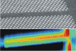
The team made a lattice of smooth gold bumps 400 nm apart on a gold surface but left bump-free channels through the lattice to serve as wave guides. They created SPPs by aiming near infrared laser light at a standard light-to-SPP coupling device on the surface and detected them using a scanning near-field optical microscope (SNOM). The SNOM’s glass fiber tip picks up a small leakage of electromagnetic waves as it’s scanned across the surface to build up an image.
The images show that 782-nm-light-induced SPPs cannot penetrate into the periodic structure, whereas at somewhat longer wavelengths, they do penetrate. Bozhevolnyi calls this steep wavelength dependence “smoking gun evidence” of the band gap effect. Other images show SPPs traveling along waveguides, although not quite the way the team expected. “We did not know that one should be careful with the width of the channel,” Bozhevolnyi admits, because theorists have not yet tackled this challenging problem.
But soon they will, says Alexei Maradudin of the University of California at Irvine. “It’s a clever idea [that] I’m sure will stimulate theoretical work,” he says, adding that the paper has got him thinking about doing some related calculations. William Barnes of the University of Exeter in the U.K. and Maradudin believe that SPP photonic structures may be important for devices in the future, but Barnes is also interested in the basic physics. “The interaction between surface plasmon modes and periodic structures is full of unanswered questions,” he says.


