Convincing a magnetic semiconductor to work at room temperature
Magnetoelectronics—electronics that make use of the magnetic (spin) property of the charge carriers—has revolutionized the information storage industry over the past two decades. However, in doing so it has also created a new bottleneck in the process of handling information. Storage is done in metal-based magnetic devices, whereas information processing is optimally realized using semiconductor devices [1]. The exchange of information between these two segregated systems is both energy and time consuming. Significant gain would be achieved if storage and processing could be brought together on a single chip. Semiconductor spintronics is the extension of magnetoelectronics to the realm of magnetic semiconductors. It combines all properties needed for both storage and processing of information in one material, and therefore is a promising solution to the component segregation issue. It would not be unexpected if it also led to fundamentally new information-processing paradigms.
The primary practical challenge to the commercialization of magnetic semiconductor spintronic devices is their operation temperature. The onset of ferromagnetism in a material occurs at its Curie temperature, but so far, a magnetic semiconductor with a Curie temperature above 200 K has not been found. Hybrid ferromagnetic metal/ferromagnetic semiconductor structures are promising possibilities for overcoming this obstacle. In such devices, the ferromagnetic properties of a metal with a Curie temperature well above room temperature are used to enhance the magnetic properties of the semiconductor. In a paper appearing in Physical Review Letters, Francesco Maccherozzi and colleagues at the TASC National Laboratory in Trieste, Christian Back and colleagues at the Institute for Experimental Physics in Regensburg, and collaborators in Germany, Switzerland, and Italy [2] make significant progress in understanding the nature of the magnetic interaction between the metal and the semiconductor in such hybrid structures. While in their current investigation the metal’s influence was limited to a small fraction of the semiconductor layer, they report a magnetic proximity effect that will be a key step towards the goal of using metals to influence the magnetic behavior of a complete functional device.
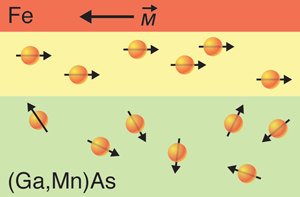
Maccherozzi et al. study a hybrid system comprised of a layer of iron, grown over doped with magnetic manganese impurities, (see Fig. 1). Their choice of materials is well motivated by the state of the art in the field. is the prototypical ferromagnetic semiconductor, and it has been extensively characterized with optical, transport, magnetic, structural, and growth studies over the past decade. It is based on the semiconductor , in which only a few percent of the gallium atoms are replaced with manganese, and therefore retains much of the structural properties. When looking for a ferromagnetic metal to pair with , it is quite natural to turn to iron. Iron has a cubic lattice structure and is nearly lattice-matched to , allowing for it to be grown either in polycrystalline form or with its crystal structure matching that of the underlying (epitaxially), depending on the growth conditions. The magnetic properties of hybrid structures have been characterized extensively [3] and it is known that in such hybrids the iron in its epitaxial form exhibits many of the same magnetic anisotropy properties as . Therefore, the probability is high that the ferromagnetic states of iron and are compatible to cooperate with each other.
Maccherozzi et al. examine the device primarily with x-ray absorption spectroscopy and x-ray magnetic circular dichroism (XAS and XMCD) [4]. The x-ray absorption spectrum is typically comprised of multiple absorption peaks corresponding to the energy required to excite the core electrons between various shells of the atom of a specific element. It is possible, for example, to tune the energy range of the x rays and thereby focus on the L-edge of iron and manganese corresponding to a transition from 2 to 3 orbitals. XMCD is an extension of XAS in which the polarization of the light is taken into account. In magnetic atoms, the shell contains an unequal amount of spin-up versus spin-down electrons, which results in different absorption cross sections for right- and left-hand circularly polarized photons. By measuring the change of polarization in an x-ray beam after it traverses the system, it is possible to extract the amplitude and direction of the average magnetization of a given atomic species.
As a result of their studies, Maccherozzi et al. reach two important conclusions regarding the nature of the ferromagnetic metal/ferromagnetic semiconductor interface. First, there is no magnetically “dead” layer at the interface. That is an important finding, as it can often happen that when a ferromagnetic metal is grown on a semiconductor or insulator, a thin layer of the order of a nanometer on the magnetic side of the interface loses its ferromagnetic character. Second, a proximity effect induced by the iron layer (red region in Fig. 1) mediates an alignment of the free magnetic moments in a layer at the interface, extending approximately 2 nm into (yellow region in Fig. 1). Ab initio and Monte Carlo calculations support these results and confirm that the strong exchange coupling parameter in the iron acts to stabilize a ferromagnetic exchange interaction in the semiconductor, leading to a region of about four monolayers where the effective Mn-Mn interaction is ferromagnetic in nature. Simultaneously, an antiferromagnetic coupling between that thin layer and the bulk of the iron is created, which results in the magnetization of the layer being opposite to that of the iron, as shown in Fig. 1.
This result bodes well for plans to use ferromagnetic metals to influence the magnetic state of magnetic semiconductors. Although the direct proximity effect is limited to a thin layer, once the magnetic semiconductor is in a ferromagnetic state, the stiffness of that state (the reluctance to spontaneously nucleate domains with different magnetizations) will naturally extend the range of the interaction. Therefore, if the proximity effect could be implemented in a scheme where one is operating below the effective Curie temperature of the coupled magnetic semiconductor layer, the possibility of using it as an effective device element is quite promising. Indeed, our interest in this work is partially motivated by our own recent work, which is attacking the same issue from the opposite direction. In recent experiments [5], we have witnessed an interesting interplay between permalloy/ hybrid structures investigated well below the natural Curie temperature of . We find that despite the magnetic coupling caused by the direct proximity of the two layers, they retain their individual character, and their relative alignment can be controlled by an external magnetic field. However, the microscopic origin of the magnetic interaction through the interface remains unclear.
In this work, Maccherozzi et al. have made great strides in elucidating the nature of the interaction through such interfaces, at least above the Curie temperature of . Merging both this work and low-temperature-device investigations seems to be the optimal course of action towards understanding these fascinating magnetic metal/semiconductor hybrid systems.
References
- David D. Awschalom and Michael E. Flatté, Nature Physics 3, 153 (2007)
- F. Maccherozzi, M. Sperl, G. Panaccione, J. Minár, S. Polesya, H. Ebert, U. Wurstbauer, M. Hochstrasser, G. Rossi, G. Woltersdorf, W. Wegscheider, and C. H. Back, Phys. Rev. Lett. 101, 267201 (2008)
- R. P. Cowburn, S. J. Gray, J. Ferré, J. A. C. Bland, and J. Miltat, J. Appl. Phys. 78, 7210 (1995)
- G. Schütz, E. Goering, and H. Stoll, in Handbook of Magnetism and Advanced Magnetic Materials, edited by H. Kronmller and S. Parkin (John Wiley & Sons, Ltd., 2007), Vol 3, p. 1309[Amazon][WorldCat]
- S. Mark, C. Gould, K. Pappert, J. Wenisch, K. Brunner, G. Schmidt, and L. W. Molenkamp, arXiv:0812.0455 (2008)


