How to Make Devices with Weyl Materials
In 2015, physicists discovered a new topological state of matter known as a Weyl semimetal. Electronic excitations in such a material do not behave as nearly free electrons, like in most metals. Instead, they can effectively be described as massless relativistic particles with properties similar to photons. Beside their fundamental interest, the exotic behavior of Weyl fermion materials motivates the pursuit of electronic or optical devices with novel functionalities. Romilly Hills at Loughborough University, UK, and collaborators have now theoretically investigated a range of devices that could be made using such materials [1]. In particular, they propose that a structure made of multiple layers of Weyl semimetals would behave as a medium whose effective refractive index is negative, which could focus a diverging electron beam onto an extremely small region. Such a property could lead to a “superlens” that boosts the spatial resolution of scanning tunneling microscopes (STMs).
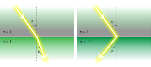
In 984, the Persian scientist Ibn Sahl showed that the bending of light as it passes from one medium to another is governed by the two media’s indices of refraction—a relation known more familiarly today as Snell’s law. Typical materials, like water or air, have a positive index, meaning that the angle of transmission, as measured between the normal and the interface between the two media, is always positive (see Fig. 1, left). In this case, light refraction creates familiar optical effects like the bending of a straw in a glass of water. In 1967, however, the physicist Viktor Veselago showed that a negative index of refraction would lead to unconventional optical properties [2]: the transmission angle would become negative (see Fig. 1, right) such that diverging light rays would be focused. In other words, a slab of negative-index material acts as a lens. In 2000, John Pendry suggested that such a Veselago lens, or “hyperlens,” could bypass the limits posed by diffraction, allowing optical microscopes to probe subwavelength objects [3].
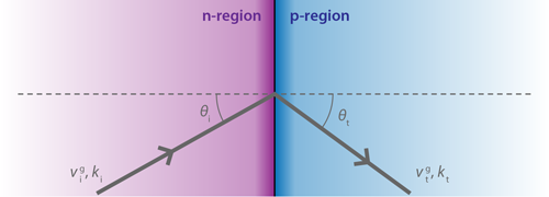
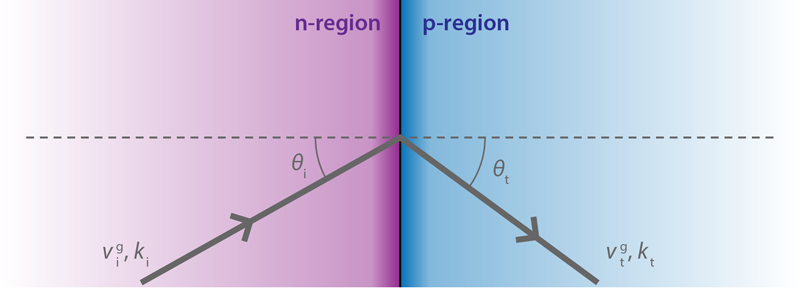
Realizing a medium with negative refraction is challenging. For photons, this behavior has been achieved using artificial metamaterials that work at microwave and visible wavelengths. The main proposal of Hills et al. is that Weyl semimetals could be used to realize a Veselago lens for electrons. The result builds on earlier work on graphene, the one-atom-thick carbon layer whose electrons also behave as massless relativistic particles. In 2007, Cheianov et al. [4] predicted that electrons propagating through a potential barrier in graphene behave as light waves that have been transmitted into a medium with a negative refractive index. This occurs because the group velocity of charged massless relativistic particles can be parallel or antiparallel to their momentum, depending on their charge. Hence, when an electron wave is transmitted through an n-p junction, that is, from an n-type (electron dominated) region into a p-type (hole dominated) region, the group velocity switches sign. At the same time, the momentum tangential to the interface must be preserved. Together, these two conditions imply that the ratio of the incident to transmitted momenta is negative, resulting in an effective refraction index that’s negative. Cheianov et al.’s proposal was experimentally realized in 2015 [5], providing a two-dimensional electronic realization of the Veselago lens.
Hills and collaborators now show that the mechanism described by Cheianov et al. also works in a three-dimensional Weyl semimetal. The team first analyzes a heterostructure made of two Weyl semimetals, such as NbAs and NbP, calculating the transmission probability of an electron current impinging on the interface at a certain angle (see Fig. 2). The resulting transmission curve is similar to that seen in graphene, indicating a negative refractive index behavior. This result confirms a previous theoretical study on layered Weyl semimetal structures [6], which, however, was primarily focused on how an applied magnetic field affects electron transmission.
Building on this conclusion, the authors go on to design a three-dimensional Veselago lens made of three layers of different Weyl materials, suggesting that such a lens can be used as a probing tip for STMs. Current STMs use a sharp metallic tip to focus an electron beam onto a sample. Since STM’s imaging resolution is limited by the tip’s geometry and imperfections, it ultimately depends on the tip manufacturing process, which today remains a specialized art, unsuitable for mass production. According to Hills et al., replacing the STM tip with their multilayer Weyl structure would result in a STM whose spatial resolution is limited only by how accurately the electron beam can be focused through Veselago lensing. A STM designed in this way could focus electron beams onto sub-angstrom regions, which would boost STM’s precision to levels at which the technique could routinely see individual atomic orbitals and chemical bonds.
Further theoretical and experimental work is needed to establish whether the authors’ predictions are reliable. The team considers an idealized model of Weyl semimetals, whereas similar research in graphene warns of the effect of potential departures from idealized conditions. For instance, deviations from perfect relativistic behavior can cause aberrations in a graphene-based lens [7]. The effect of disorder or of the interface’s smoothness should also be investigated. In addition, it is not clear whether an effective description in terms of Weyl fermions is justified at the sub-angstrom scales where the electron beam would be focused. Finally, a more complete theoretical description will need to incorporate, in addition to bulk Weyl states, the topologically protected Weyl states that may exist at the interfaces between materials [8]. On the positive side, it should be possible to test the new predictions using the optical analogs of Weyl materials realized in photonic crystals [9].
The authors explore two additional potential applications of Weyl semimetals. First, they analyze a transistor in which a Weyl semimetal replaces the conventional semiconductor material. The figures of merit of such a Weyl transistor, the authors argue, may be comparable to those of the graphene-based transistors that are being considered for post-silicon electronics. Second, they suggest that an applied pressure can drive the Weyl phase into a phase known as a type-II Weyl semimetal. Type-II Weyl fermions [10] bear similarities to light moving in an extremely distorted spacetime environment—a situation that would be reminiscent of a black hole’s environment.
The proposal by Hills et al. is an encouraging first step towards the realization of Weyl-based devices and may open the door to new physics. An example is the idea of Weyl metamaterials [11], which can be engineered by modulating strain within a Weyl or Dirac material. Such metamaterials can exhibit propagation features that include Veselago lensing but may have further reaching consequences [12]. For instance, certain geometries can transmit the two chiral “flavors” of Weyl fermions in two different ways (Weyl fermions can be either left handed or right handed). Such a behavior can be used to realize chirality filters, the first step towards chiraltronics—an alternative to spintronics in which information is encoded in the carriers’ chirality.
This research is published in Physical Review B.
References
- R. D. Y. Hills, A. Kusmartseva, and F. V. Kusmartsev, “Current-Voltage Characteristics of Weyl Semimetal Semiconducting Devices, Veselago Lenses and Hyperbolic Dirac Phase,” Phys. Rev. B 95, 214103 (2017).
- V. G Veselago, “The Electrodynamics of Substances with Simultaneously Negative Values of and ,” Sov. Phys. Usp. 10, 509 (1968).
- J. B. Pendry, “Negative Refraction Makes a Perfect Lens,” Phys. Rev. Lett. 85, 3966 (2000).
- V. V. Cheianov, V. Fal, and B. L. Altshuler, “The Focusing of Electron Flow and a Veselago Lens in Graphene p-n Junctions,” Science 315, 1252 (2007).
- G. H. Lee, G.-H. Park, and H. J. Lee, “Observation of Negative Refraction of Dirac Fermions in Graphene,” Nat. Phys. 11, 925 (2015).
- C. Yesilyurt, S. G. Tan, G. Liang, and M. B. A. Jalil, “Klein Tunneling in Weyl Semimetals under the Influence of Magnetic Field,” Sci. Rep. 6, 38862 (2016).
- K. J. A. Reijnders and M. I. Katsnelson, “Diffraction Catastrophes and Semiclassical Quantum Mechanics for Veselago Lensing in Graphene,” arXiv:1703.07769.
- A. G. Grushin, J. W. F. Venderbos, A. Vishwanath, and R. Ilan, “Inhomogeneous Weyl and Dirac Semimetals: Transport in Axial Magnetic Fields and Fermi Arc Surface States from Pseudo-Landau Levels,” Phys. Rev. X 6, 041046 (2016).
- Z. Wang, D. Ye, L. Ran, L. Fu, J. D. Joannopoulos, and M. Soljačić, “Experimental Observation of Weyl Points,” Science 349, 622 (2015).
- A. A. Soluyanov, D. Gresch, Z. Wang, Q. Wu, M. Troyer, X. Dai, and B. A. Bernevig, “Type-II Weyl Semimetals,” Nature 527, 495 (2015).
- A. Weststrom and T. Ojanen, “Designer Curved-Space Geometry for Relativistic Fermions in Weyl Metamaterials,” arXiv:1703.10408.
- C.-X. Liu, P. Ye, and X.-L. Qi, “Chiral Gauge Field and Axial Anomaly in a Weyl Semimetal,” Phys. Rev. B 87, 235306 (2013); A. Cortijo, Y. Ferreirós, K. Landsteiner, and M. A. H. Vozmediano, “Elastic Gauge Fields in Weyl Semimetals,” Phys. Rev. Lett. 115, 177202 (2015); D. I. Pikulin, A. Chen, and M. Franz, “Chiral Anomaly from Strain-Induced Gauge Fields in Dirac and Weyl Semimetals,” Phys. Rev. X 6, 041021 (2016).


