Double or nothing for spin filters
In the last twenty years, control of the electron spin in electrical transport has advanced to the point where it now has serious application in data storage and magnetic sensing [1]. Additionally, this growing field is becoming increasingly cross disciplinary. When viewed next to control of charge in semiconductor-based devices, the manipulation of the electron spin remains a challenge, with researchers striving towards new approaches that lead to functional use.
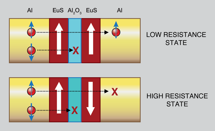
In a paper appearing in Physical Review Letters, Guo-Xing Miao, Martina Müller, and Jagadeesh Moodera, at Massachusetts Institute of Technology have given experimental evidence for a sizeable magnetoresistive (MR) effect—a relative change of resistance with magnetic field—in a tunnel-junction device consisting of two decoupled magnetic barriers sandwiched between two nonmagnetic electrodes [2]. The magnetic insulating material filters the spin direction of the electron current tunneling through the device (see Fig. 1). The great potential of the configuration used by Miao and co-workers was theoretically predicted a few years ago by D. C. Worledge and T. H. Geballe at Stanford University [3]. Even though the result reported by Miao et al. is a proof-of-concept, only working at low temperatures, it is a step towards future applications in data storage and magnetic sensing, if the device can be grown with appropriate materials.
What is meant by tunneling in this case? In a tunnel junction, a small but significant portion of an incoming electron current from one electrode can tunnel through an insulating material to a second electrode, provided that the insulating barrier thickness is no thicker than a few nanometers. The electron preserves its spin direction during tunneling, so if one uses magnetic electrodes, the resistance of the device depends on the magnetic orientation of the electrodes [4]. As a consequence, the tunneling probability of an electron coming from the first electrode will depend on the available density of states with the same spin direction in the second electrode. Bearing this in mind, and considering the imbalanced number of spin-up and spin-down electrons due to the first magnetic electrode, we see that the current flowing depends strongly on whether the magnetic electrodes are parallel or antiparallel. Initially only moderate MR values were found in such magnetic tunnel junctions, but subsequently large MR effects (approaching 500%) at room temperature in Fe/MgO/Fe-type tunnel junctions [5] paved the way for their quick implementation in magnetic read heads and magnetic sensors in 2005, replacing fully metallic giant-magnetoresistance devices [1].
The phenomenon of spin filtering and the corresponding MR effect is also observed in tunnel-junction devices, but here the main mechanism is different from that in magnetic tunnel junctions. In this case, the insulating barrier is a ferromagnetic insulator, which filters selectively one of the two electron spin directions [6]. Due to the exchange interaction in ferromagnetic materials, the conduction band in the ferromagnetic insulator is split into two subbands (spin-up and spin-down) separated by the exchange splitting energy. The result is that if an electron tunnels through such ferromagnetic barrier, the barrier height it experiences will depend on the orientation of its spin with respect to the magnetization direction of the barrier. One advantage of the spin-filter mechanism is that the tunneling is very sensitive to the applied voltage, which is very useful for microelectronic applications.
The first experimental demonstration of spin filtering dates back to 1972, when Müller et al. found that electrons emitted from tungsten tips covered by EuS presented a high spin polarization of 89% [7] (the spin polarization is the percentage of spin-up electrons compared to the total number of electrons). EuS is indeed an efficient spin-filter material, which has been used in quasimagnetic tunnel junctions, where the magnetic barrier is sandwiched between a magnetic electrode and a nonmagnetic electrode, producing a significant MR effect [8]. However, EuS has quite a low Curie temperature (16.6K), above which its spin-filter property disappears. This is why researchers are working hard to find spin-filter materials with Curie temperature above room temperature. The most promising candidates are ferrites such as NiFe2O4 and CoFe2O4, where small but promising MR effects have been observed in quasimagnetic tunnel junctions [9,10].
It is most interesting that in the new double spin-filter tunnel junctions reported by Miao et al. [2], no magnetic electrode is required. The two magnetic barriers act as spin-polarizer and spin-analyzer respectively. As predicted, and in sharp contrast to standard magnetic tunnel junctions, the maximum MR effect does not occur at low applied voltage but at rather large voltage (∼1V), at which point the voltage exceeds the spin-up barrier height and spin-up electrons flow easily through the magnetic barrier, whereas spin-down electrons cannot do so. This is very exciting for applications: in order to obtain large voltage output in devices it is necessary to apply high working voltages. On the other hand, a drawback from using two insulating barriers is that the final device resistance is high, a few MΩ [2], which will produce large thermal noise. The next challenge in working with these double spin filters is to grow very thin spin-filter layers to realize low-resistance devices that have a high Curie temperature enabling room-temperature operation.
Some unexplained features in the results presented by Miao et al. [2] suggest that not everything is fully understood from the theoretical point of view. The quite efficient but relatively simple theoretical treatment used to interpret the results suggests that a deeper understanding of the phenomenon is still required. This is reminiscent of the state-of-the-art of magnetic tunnel junctions at the end of the nineties, at a time before the discovery of important factors like interface effects [11] or electron wave-function symmetry effects [5,12]. There is every reason to be optimistic that new experimental results and more rigorous theoretical treatments will shed more light on the exciting physics shown by these spin-filter devices.
Even if the most straightforward applications of these spin-filter tunnel junctions might be in data storage and magnetic sensing, other technologies can benefit from them. Foremost could be the fabrication of hybrid systems in combination with semiconductors, giving rise to spin-dependent Schottky barriers for efficient spin injection [13]. Much attention is currently devoted to spin injection in semiconductors for spintronics, for which such hybrid systems remain basically unexplored. An interesting proposal for a spin-filter transistor gives an example of the possibilities [14]. The work by Miao et al. [2] is a further step in the control and manipulation of the electron spin in electrical transport by means of a double spin-filter tunnel junction, which expands the research horizons in the fields of magnetic storage, magnetic sensing, and spintronics. However, much experimental effort is still required to achieve functional devices at room temperature.
References
- A. Fert, Rev. Mod. Phys, 80, 1517 (2008)
- G-X. Miao, M. Müller, and J. S. Moodera, Phys. Rev. Lett. 102, 076601 (2009)
- D. C. Worledge and T. H. Geballe, J. Appl. Phys. 88, 5277 (2000)
- M. Julliere, Phys. Lett. A, 54 225 (1975)
- M. Bowen et al., Appl. Phys. Lett. 79, 1655 (2001); S. Yuasa et al., Nature Mater. 3, 868 (2004); S. S. P. Parkin et al., 3, 862 (2004)
- For a recent review, see J. Moodera, T. S. Santos, and T. Nagahama, J. Phys. Condens. Matter 19, 165202 (2007)
- N. Müller, W. Eckstein, W. Heiland, and W. Zinn, Phys. Rev. Lett. 29, 1651 (1972)
- P. LeClair et al., Appl. Phys. Lett. 80, 625 (2002); T. Nagahama, T. S. Santos, and J. S. Moodera, Phys. Rev. Lett. 99, 016602 (2007)
- U. Lüders et al., Adv. Mater. 18, 1733 (2006)
- M. G. Chapline and S. X. Wang, Phys. Rev. B 74, 014418 (2006); A. V. Ramos et al., Appl. Phys. Lett. 91, 122107 (2007)
- J. M. De Teresa et al., Science 286, 507 (1999)
- W. H. Butler et al., Phys. Rev. B 63, 054416 (2001); J. Mathon and A. Umerski, 63, R220403 (2001)
- W. A. Thompson et al., Phys. Rev. Lett. 26, 1308 (1972); C. Ren et al., Appl. Phys. Lett. 86, 012501 (2005)
- S. Sugahara and M. Tanaka, Physica E 21, 996 (2004)