Are we seeing atoms diffuse?
Following the path of a single atom or point defect as it diffuses inside a solid remains one of the most sought after but undemonstrated feats of microscopy. In a paper in Physical Review B, Damien Alloyeau, Sefa Dag, Lin Wang, and Christian Kisielowski at the Lawrence Berkeley National Laboratory in the US, and Bert Freitag at FEI Company in the Netherlands report their use of one of the new aberration-corrected transmission electron microscopes and claim to have imaged the three-dimensional positions of Ge self-interstitials generated by the beam [1]. Have they finally succeeded in imaging diffusion?
Atomic motion on surfaces has been studied via scanning probe investigations such as atomic force microscopy and scanning tunneling microscopy. And imaging collections of impurities or point defects inside solids, such as particles of a second phase, vacancy clusters (voids), lines of point defects (dislocations), or arrays of point defects (for example, in substoichiometric oxides) is feasible and commonly demonstrated by conventional transmission electron microscopy [2,3]. Large enough collections of defects are associated with strain fields that cause variations in the diffraction amplitudes that are easily visible. The motion of dislocations and precipitates inside solids can also be monitored in situ. It is the detection of an individual impurity, vacancy, or interstitial, or a small cluster of these defects in a solid, and their motion inside the solid that is still challenging.
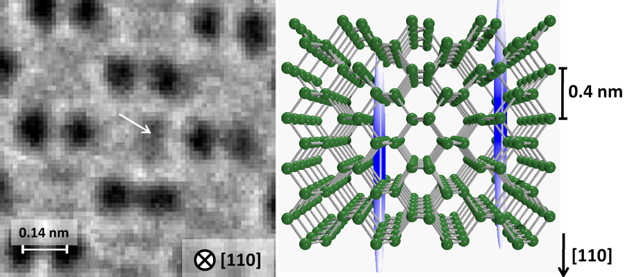
Instruments are being continually improved, however, and atomic resolution electron microscopy may soon need a name change to subatomic microscopy [4]. The instrumental resolution [5] of the aberration-corrected microscope used in this work (the TEAM 0.5 facility) is below 0.5nm (Fig. 1). Similar microscopes elsewhere will duplicate or further reduce this number soon if they have not already. Such microscopes utilize electron beams generated by a field emission gun (FEG). These very bright, very small, and highly coherent sources have their own history of development and come in a few varieties, but it was the combined attention to improvements in the other components of a transmission electron microscope (TEM) that has gradually allowed their capabilities to be fully exploited. Isolation of the sample and microscope from any sources of mechanical vibration, electrical noise, and stray magnetic fields has always been important but the sensitivity of these new instruments now requires the careful design of the entire building that houses the microscope as well as all facilities and systems attached to the microscope.
The authors’ choice of an acceleration voltage of 300kV is a compromise between sample damage from electron-nuclear collisions (beginning at about 350keV in the case of Ge) and resolution. Higher electron energies, and thus smaller wavelengths, give higher resolution based on diffraction and the Raleigh criteria familiar in optics. For a given wavelength, a wider electron beam area or shorter focal length would also normally improve resolution. Instead, electromagnetic lenses in any TEM, even under the best manufacturing conditions, suffer from spherical aberration or the inability to focus electrons to the same spot for all incident angles. It is the spherical aberration coefficient of the objective lens (a third-order coefficient usually given the symbol Cs) that has limited resolution, at least up until a few years ago. Thus in conventional TEMs, image quality improves for smaller beam diameters with an aperture inserted before the sample to reduce the solid angle subtended by the beam.
The new microscopes have spherical aberration correctors. That means that there is a system of extra fields that reduces Cs to negligible values. The development of these corrector systems are to a point where reducing the fifth-order spherical aberration coefficient is now a measure of progress [6]. At 300kV the electron wavelength is 0.0019nm and hence a resolution limited by diffraction might be about 0.001nm. The measured resolution demonstrated for this microscope is only 0.05nm so there is still potentially 50 times better resolution theoretically feasible, but other issues also limit resolution.
Note that the samples in this work were exquisitely thin, 1–2 nm, only five {110} atomic planes in thickness. Besides electrical, mechanical, or magnetic noise, the energy width ΔE of the beam will limit resolution due to chromatic aberration (i.e., errors in focusing electrons of different wavelengths). The monochromator reduced ΔE to 0.2eV, but as the beam passes through the sample it loses energy to various processes and ΔE increases again. Thin samples are thus necessary to reduce this effect.
Thin samples are also important when analyzing the images obtained. In this experiment the researchers aimed a fixed electron beam at the crystalline sample. The beam diameter might have been 100nm or less. This produced an image consisting of a set of interference fringes related to the lattice period, and with the aberration corrector the fringes are sharper. Like a multiple slit experiment, the lateral atomic positions are not reliably correlated with the fringe positions. For some focus conditions the spots are black while in others they are white. This contrast reversal is a common phenomena—an indication that the atom positions are not directly known. In order to reconstruct the structure of the sample, the standard solution for some time has been to take a set of images through the focus and to simulate each image with the known set of sample and microscope parameters [7]. The sample structure is reconstructed with all images contributing. This was carried out in this experiment and works well for the lattice atoms. However, the interstitial atoms are not static, nor periodic.
Others have imaged static interstitials in certain systems using aberration-corrected scanning TEM (STEM), whereby the small focal spot of the FEG source is scanned laterally across the sample. The same aberration-corrected subangstrom probe can be aimed in between rows of atoms of a suitably aligned single crystal, thus probing the mass density as a function of lateral position. The interaction of the beam with the sample becomes relatively simple and straightforward to interpret. Essentially like Rutherford backscattering analysis of ion scattering, the probability of electron scattering increases as the atomic number squared. Combining through-focus image analysis in a STEM, the location of point defects have been determined. In this way, researchers have been able to image individual substitutional Sb atoms inside Si [8], Hf atoms inside an amorphous SiO2 layer [9], Au interstitials inside a Si nanowire [10], and Ca vacancies within Ca0.33CoO2 [11]. These investigations all relied on the impurity atoms or vacancies remaining static during the image collection. The same set of through-focus images could be collected more than once from the same area, increasing our confidence in their conclusions. But the large mass difference between the impurity or vacancy and matrix was critical to the contrast. This approach may not yet have the sensitivity to detect these Ge interstitials.
In this work, Ge interstitial defects apparently formed via electron irradiation due to their proximity to the surface. The images obtained relied on an interstitial atom remaining relatively still for a large fraction of a second. Unfortunately, the same interstitial could not be imaged more than once, since they moved faster than the image collection rate. It is true that there is a remarkably low level of noise between their spots and if we are going to image diffusing atoms they will need to be random and moving. However, to be convinced that we are really seeing interstitials, we need a faster acquisition time or a more static point defect and then need to follow the subsequent movements of these objects individually.
The work reported in the paper by Alloyeau et al. is a remarkable demonstration of the capabilities of the latest TEMs. They are very close to having a convincing case that they have imaged diffusing point defects. Soon, no doubt, the right combination of defect stability and beam or thermally induced diffusion control will finally let us see atomic diffusion.
References
- D. Alloyeau, B. Freitag, S. Dag, L. W. Wang, and C. Kisielowski, Phys. Rev. B 80, 014114 (2009)
- P. Hirsch, Electron Microscopy of Thin Crystals (Kreiger, Malabar, FL, 1965)[Amazon][WorldCat]
- K. L. Kavanagh, C. W. McGee, J. Sheets, and J. W. Mayer, J. Appl. Phys. 64, 1845 (1988)
- R. Erni, M. D. Rossell, C. Kisielowski, and U. Dahmen, Phys. Rev. Lett. 102, 096101 (2009)
- David J. Smith, Ultramicroscopy 108, 159 (2008)
- C. Kisielowski et al., Microsc. Microanal. 14, 469 (2008)
- W. Coene, G. Janssen, M. Op de Beeck, and D. van Dyck, Phys. Rev. Lett. 69, 3743 (1992)
- P. M. Voyles, J. L. Grazul, and D. A. Muller, Ultramicroscopy 96, 251 (2003)
- K. van Benthem, A. R. Lupini, M. Kim, H. S. Bauk, S. Doh, J.-H. Lee, M. P. Oxley, S. D. Findlay, L. J. Allen, J. T. Luck, and S. J. Pennycook, Appl. Phys. Lett. 87, 034104 (2005)
- S. H. Oh, K. Van Benthem, S. I. Molina, A. Y. Borisevich, W. Luo, P. Werner, N. D. Zakharov, D. Kumar, S. T. Pantelides, and S. J. Pennycook, Nano Lett. 8, 1016 (2008)
- Rong Huang, Teruyasu Mizoguchi, Kenji Sugiura, Hiromichi Ohta, Kunihito Koumoto, Tsukasa Hirayama, and Yuichi Ikuhara, Appl. Phys. Lett. 93 181907 (2008)