Spin Hall effect goes electrical
In an analogy with psychoanalysis, it can be said that today’s technology exploits the dual personalities of the electron, one negative (its charge) and one antisocial (its spin 1/2), and that these are usually considered separately. The first makes it easy to generate charge flow and logic devices via electric fields. The latter is responsible for ferromagnetism (together with the Coulomb interaction), which dominates information storage technologies. The link between these two personalities is the spin-orbit coupling, which is a weak interaction in solids because of its relativistic nature. Though weak, the spin-orbit coupling can have profound consequences for materials properties and is the source of several, potentially technologically useful, effects.
One such effect that has been a very active focus of study over the past few years is the spin Hall effect. This effect occurs when an unpolarized charge current traverses a material with spin-orbit interaction, leading to a perpendicular spin current where “up” spins accumulate on one edge of the sample and “down” spins accumulate on the other. Although the spin Hall effect was predicted over three decades ago [1], it received little attention until studies on the intrinsic nature of its ferromagnetic cousin, the anomalous Hall effect (an additional contribution to the Hall resistivity in magnetic materials), led to the prediction of a similar large spin Hall effect in strongly spin-orbit coupled materials [2,3]. The intense theoretical debate that ensued, and which still remains, to a degree, fueled the need for experimental verification of the effect itself. This came through two key optical experiments, one utilizing the Kerr-microscopy technique in electron systems with weak spin-orbit coupling [4], and the other using a two-dimensional light-emitting diode technique in hole-doped semiconductors with strong spin-orbit coupling [5]. However, because this spin accumulation does not directly lead to a charge Hall voltage, most of the studies have been restricted to optical measurements [6–8]. The scarcity of experiments done so far, and the limited materials range studied up to now, means many questions remain on the effect itself, its specific origin, and its consequences for other systems and related effects.
Now, however, Eric Garlid and colleagues at the University of Minnesota, in collaboration with the University of California, Santa Barbara, both in the US, report in Physical Review Letters on the direct detection of the spin Hall effect through transport electrical measurements [9]. They have succeeded in doing this by adapting previous techniques of spin-transport in ferromagnet-semiconductor devices [10] to the present experiment. This experiment also systematically studies the spin Hall effect as a function of the spin-orbit coupling strength, adding to the much-needed quantitative analysis of this effect. This new technique opens the door to other materials where optical measurements are not possible and, by being more widely accessible, allows more teams to participate in this field.
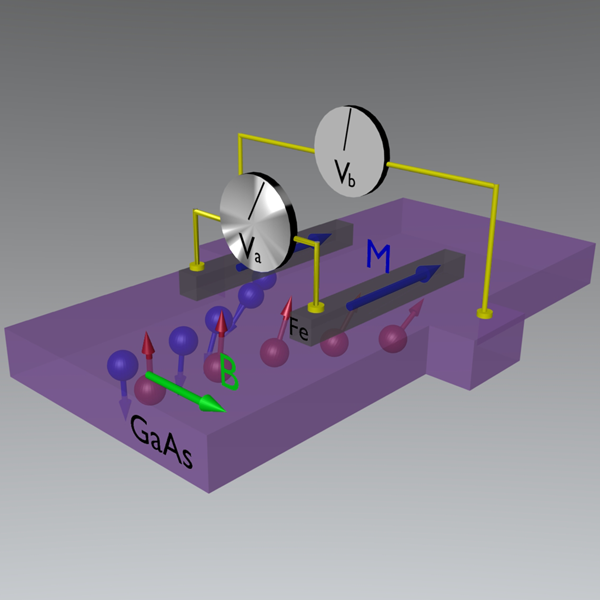
Garlid et al. study the effect in a series of samples of InxGa1-xAs with two ferromagnetic contacts on the edges of the sample and a weak magnetic field along the sample in the direction shown in Fig. 1. This transverse magnetic field results in a precession of the spin-accumulation so that it acquires a component parallel to the magnetization direction of the contacts. In combination with spin relaxation, the resulting field-dependence of the voltage difference between the ferromagnetic contacts is known as the Hanle effect [11]. In this regime of relatively weak spin-orbit coupling, the distinct shape of the Hanle curve distinguishes the signal from the backgrounds. Although other unrelated magnetoresistance signals are present in the direct measurement, the authors exploit the symmetry of the effect to extract the direct contribution from the spin-Hall effect and are able to measure to a relatively good accuracy the spin-Hall conductivity inferred from the spin-accumulation measured [9].
One key aspect of this experiment is that Garlid et al. are able to tune the strength of the spin-orbit interaction between different samples by changing the indium doping, as well as the conductivity of each sample. This allows them to extract the different contributions to the spin Hall conductivity, since they can be characterized by their dependence on these parameters; in particular, how the spin Hall signal depends on the conductivity. Contributions to the spin Hall conductivity that are linear in the conductivity are assumed to be due to the skew scattering mechanism, while the conductivity independent contributions, i.e., scattering independent, are identified as a mixture of the side-jump and intrinsic contributions (which cannot be separated in transport experiments) and are dependent on the band structure alone for metallic systems [12].
As the strength of the spin-orbit coupling increases, one expects the spin Hall conductivity, and consequently the spin current that arises from it, to increase. At the same time, however, the spin lifetime decreases, and it is not a priori obvious whether the resulting spin accumulation should increase or decrease in any given experiment. In their experiment, Garlid et al. observe a decrease of the spin accumulation for increasing spin-orbit coupling strength [9]. The setup employed by Garlid et al. also allows one to vary the ordinary conductivity of the channel. By doing this, they extract the two contributions to the spin-Hall conductivity, which for this system have opposite sign. They show that the magnitude of each of the two contributions increases with doping at fixed conductivity of the channel. Another important finding is that the ratio of the two contributions is almost constant and independent of spin-orbit coupling strength, as expected from theory, although the measured ratio does not agree with expectations [13]. This disagreement may arise from comparing the simpler theory in the metallic regime to the experiment, which is in a more disordered regime close to the metal insulator transition but in the metallic side. As expected in n-doped semiconductors, the observed spin Hall conductivity is dominated by the skew scattering contribution over the scattering independent contribution.
The results hint to the resolution of a puzzling result from a previous optical experiment in ZnSe [8], whose spin-orbit coupling is an order of magnitude lower than GaAs. In that experiment the optically measured signal was of the same order of magnitude as in GaAs and observed even at room temperature. The present results seem to indicate that, even though the spin Hall conductivity contributions may be lower in themselves, their cancelling effect may be less complete, and the resulting total spin Hall conductivity remains as strong as in GaAs. A possible alternative or additional cause is that the longer spin-lifetime leads to a larger spin-accumulation, which is at the end what is being measured, leading to an optical signal of similar strength. Further systematic studies similar to the ones in the present InxGa1-xAs study would be of great value.
The work of Garlid et al. opens new possibilities for the study of the spin Hall effect and illustrates beautifully how different techniques can be adapted to measure new effects in a systematic way. The lopsided ratio between theory and experiment in the field, due primarily to the difficulty and restrictions of the optical measurements, may now begin to reach a much healthier state as new materials are studied and new teams enter the field.
References
- M. I. D’yakonov and V. I. Perel, JETP Lett. 13, 467 (1971)
- S. Murakami, N. Nagaosa, and S.-C. Zhang, Science 301, 1348
- J. Sinova, D. Culcer, Q. Niu, N. A. Sinitsyn, T. Jungwirth, and A. H. MacDonald, Phys. Rev. Lett. 92, 126603 (2004)
- Y. K. Kato, R. C. Myers, A. C. Gossard, and D. D. Awschalom, Science 306, 1910 (2004)
- J. Wunderlich, B. Kaestner, J. Sinova, and T. Jungwirth, Phys. Rev. Lett. 94, 047204 (2005)
- V. Sih, R. C. Myers, Y. K. Kato, W. H. Lau, A. C. Gossard, and D. D. Awschalom, Nature Phys. 1, 31 (2005); N. P. Stern, D. W. Steuerman, S. Mack, A. C. Gossard, and D. D. Awschalom, 4, 843 (2008)
- K. Nomura, J. Wunderlich, J. Sinova, B. Kaestner, A.H. MacDonald, and T. Jungwirth, Phys. Rev. B 72, 245330 (2005)
- N. Stern, S. Ghosh, G. Xiang, M. Zhu, N. Samarth, and D. D. Awschalom, Phys. Rev. Lett. 97, 126603 (2006)
- E. S. Garlid, Q. O. Hu, M. K. Chan, C. J. Palmstrøm, and P. A. Crowell, Phys. Rev. Lett. 105, 156602 (2010)
- X. Lou, C. Adelmann, S. A. Crooker, E. S. Garlid, J. Zhang, K. S. Madhukar Reddy, S. D. Flexner, C. J. Palmstrom, and P. A. Crowell, Nature Phys. 3, 197 (2007)
- J. Fabian, A. Matos-Abiague, C. Ertler, P. Stano, and I. Zutic, Acta Physica Slovaca 57, 565 (2007)
- N. Nagaosa, Jairo Sinova, S. Onoda, A. H. MacDonald, and P. Ong, Rev. Mod. Phys. 82, 1539 (2010)
- H. Engel, B. I. Halperin, and E. I. Rashba, Phys. Rev. Lett. 95, 166605 (2005)


