Visualizing quantum mechanics
Since its invention in 1981, the scanning tunneling microscope (STM) has served as the most versatile tool for imaging individual atoms and the electronic properties of surfaces at the Ångstrom scale [1]. It has conquered the realm of nanoscale physics, where it is used to image all kinds of geometric and electronic properties found at surfaces, ranging from the intricacies of the so-called ( ) reconstruction of the surface of silicon [2] to the electronic gap in high-temperature superconductors [3]. Strictly speaking, however, the scanning tunneling microscope does not image atoms, but the perturbations they cause to the transport of charge between its probe tip and the underlying substrate. While this is often advantageous in the investigation of surface physics, chemical bonds and bonding orbitals appear only indirectly by their perturbation of the transport process. For the STM to become as useful for imaging in chemistry as in physics, it needs to reveal chemical identity, bonding, and structure in molecules.
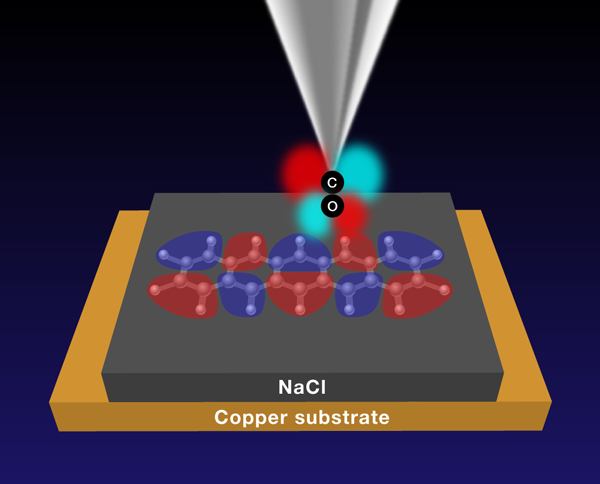
What information do chemists wish to gain? Molecular orbitals describe the spatial distribution of electrons, determining their shape and size. They derive directly from the quantum-mechanical description of molecules, and most molecular orbitals consist of multiple lobes of different sign or phase, which can be spaced quite closely. The point between the lobes, where there is zero probability of finding an electron, is known as the node. A useful way to consider the structure of a molecule is by considering the nodal planes, that is, the region of zero electron density for that orbital constructed from these nodes. A collection of nodal planes yields a nodal structure, which is vital to understanding the electronic properties of molecules. Research and commercial software for quantum mechanical modeling of molecules has generated images of nodal structures for decades, yet despite their relevance and the proven nature of the concept, they have never been seen directly before. Now, writing in Physical Review Letters, Leo Gross of IBM-Zürich, Switzerland, and collaborators have performed a new STM experiment that directly visualizes the nodal structure of molecular electronic states [4].
The path towards this experiment has gone through several stages. A sharp metallic tip providing nearly continuous, spherical, and featureless density of states for transporting electrons is—at least by itself—insufficient to reveal the sharp electronic features of molecules, and the phases of individual lobes of charge density. This prompted efforts to construct STM tips that have a well-defined atomic structure at their apex, so that the tip’s electronic structure is known. Preparing apices of metal atoms arranged in any particular setup proved difficult and the resulting apices rearranged too easily due to the malleability of metals. Inspired by prior experiments of attaching xenon atoms to the tip apex [5], at that time, I was part of a team effort trying to circumvent this problem by attaching a linear carbon monoxide ( ) molecule to the very end of an STM tip, thus creating an apex that was chemically well defined [6]. The procedure of attachment proved relatively straightforward. The capture is done by driving the STM tip over a molecule on a relatively inert metal surface, for instance copper, and tuning the voltage between tip and substrate so that the frontier or outermost orbital of , the orbital, is energetically accessible. This allows electrons of the tunneling current to populate this molecular orbital, resulting in the weakening of the CO-substrate bond. At a chance of roughly one per billion transferred electrons, the molecule-substrate bond is severed, making the molecule hop onto the tip. At a current of a nanoampere, this is accomplished in less than a second. The resulting STM tip has a molecule standing upright at its apex. There, the imparts its orbital structure on the electronic setup of the tip, foremost its frontier orbitals. This approach generated partial success in chemical imaging with -featured tips, which could distinguish between different adsorbed species, such as molecules or oxygen atoms. But resolving molecular states in the surface plane was still impossible, as here the featureless substrate electronic density still dominated.
The next idea was to put a buffer layer between the adsorbed molecule and the metal substrate, such as a clean single or double layer of an alkali-halide, for instance . Such layers electronically decouple adsorbed molecules from the substrate, allowing for the study of their electronic orbitals without interference from the substrate—as if they were freely suspended. Imaging extended molecules such as pentacene, separated by a double layer of from a copper substrate, allowed the production of stunning images of the total charge density in the molecule [7]. While definitely a step forward, the orbital geometry with its positive and negative lobes, which really govern chemical properties and intermolecular interactions, was still elusive.
With their new results, Gross et al. show that combining -functionalized tips and alkali-halide interlayers allows them to image the nodal pattern of the orbitals of flat organic molecules (Fig. 1). Here, again, the two orbitals play an important role. These derive from the orbitals of the carbon and oxygen atoms that stand perpendicular to the molecular axis. Figure 1 shows one of the orbitals: it has four lobes (drawn in red and light blue, representing their phase or sign) separated by two nodal planes. The other orbital, perpendicular to the one in Fig. 1, is not shown. By bringing the tip close to a sample molecule (pentacene in Fig. 1) separated by a salt layer from a metallic substrate, and tuning the voltage between tip and substrate to address a particular orbital of the pentacene molecule, the lobes of the orbital and those of the pentacene orbital (shown in purple and rose) come into and out of registry, as the tip is scanned across the molecule.
Transport through a multiple lobe molecular orbital and a -functionalized tip is most efficient when the phase of the tip lobes matches those of the lobes of the molecule (as shown in Fig. 1). However, if the tip is placed directly atop a lobe of the sample molecule, the transport through the lobes of different sign (red and light blue) cancel each other out, as will transport from the tip’s two lobes into sample molecule lobes of the same sign. By linking the presence or absence of signal to the position of the tip, the tip directly images the nodes of molecular orbitals and hence the orbital shape and nodal structure.
This study is not the first attempt at gaining intramolecular resolution via STM. Alternate approaches use the excitation of vibrational modes of molecules [8] and the attachment of hydrogen atoms attached to the tip apex [9]. While the former has the advantage that it can distinguish between deuterium and hydrogen and pinpoint which hydrogen atom in a molecule is actually deuterium, the latter can directly reveal the ring structure of extended aromatics without the need for insulating interlayers. None, however, have been able to reveal the nodal structure of molecular orbitals.
Gross et al.’s work will provide an important visual approach to this foundational concept of chemistry. The ability to reveal the nodal structure of molecular orbitals directly will help future generations of chemists in obtaining an intuitive understanding of molecular properties that will guide them to novel solutions in all areas of chemistry.
References
- Press Release: The 1986 Nobel Prize in Physics (http://nobelprize.org/nobel_prizes/physics/laureates/1986/press.html.
- G. Binnig et al., Phys. Rev. Lett. 50, 120 (1983)
- A. Yazdani et al., Phys. Rev. Lett. 83, 176 (1999)
- L. Gross, N. Moll, F. Mohn, A. Curioni, G. Meyer, F. Hanke, and M. Persson, Phys. Rev. Lett. 107, 086101 (2011)
- D. Eigler, C. Lutz, and W. Rudge, Nature 352, 600 (1991)
- L. Bartels, G. Meyer, and K. Rieder, Appl. Phys. Lett. 71, 213 (1997)
- J. Repp, G. Meyer, S. M. Stojkovic, A. Gourdon, and C. Joachim, Phys. Rev. Lett. 94, 026803 (2005)
- B. Stipe, M. Rezaei, and W. Ho, Science 280, 1732 (1998)
- C. Weiss et al., Phys. Rev. Lett. 105, 086103 (2010)