Landmarks—Atomic Force Microscope Makes Angstrom-Scale Images
Landmarks articles feature important papers from the archives of the Physical Review journals.
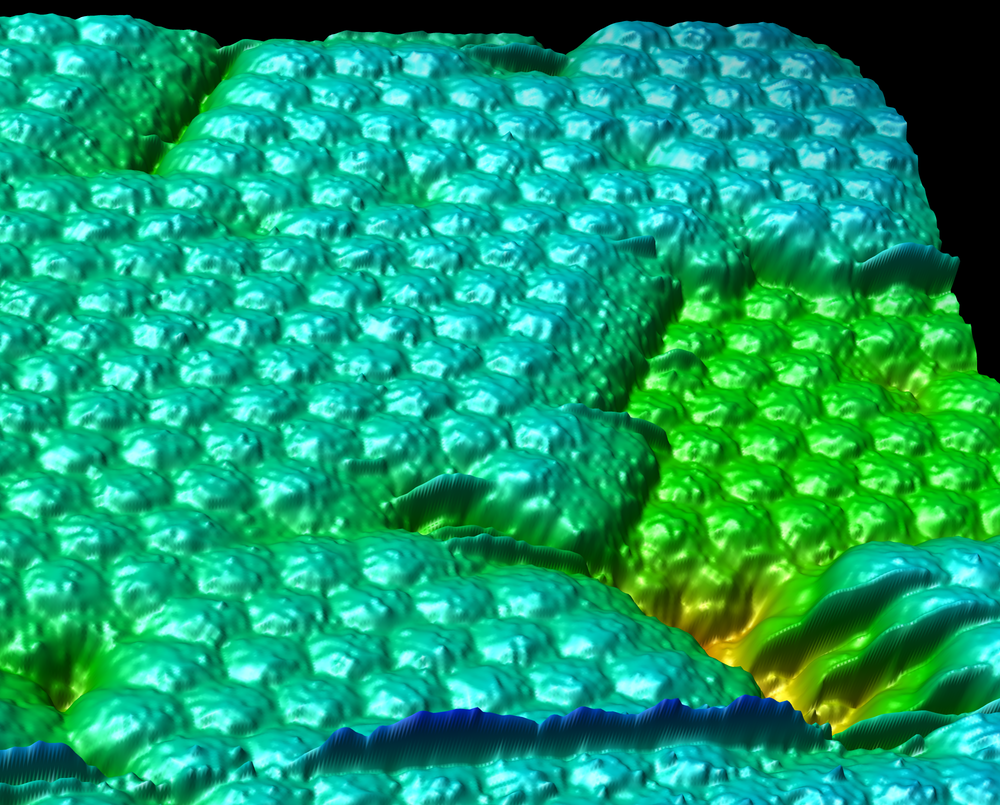
Running a finger over an irregular object is a good way to gauge its shape. In 1986, three scientists built a device to do essentially the same thing at the atomic level and published their results in Physical Review Letters. Using a tiny diamond stylus, their atomic force microscope traced out a surface with better than nanometer resolution. The device caught on quickly and with further improvements became a widely used laboratory tool for mapping surfaces with molecular precision, even for biological samples.
In 1981, Gerd Binnig and Heinrich Rohrer of the IBM Research Laboratory in Zurich invented the scanning tunneling microscope (STM). In this instrument, a sharp metal point, or “tip,” is held just above the surface of an object, close enough that a voltage induces a small current to flow across the gap between tip and surface through the phenomenon of quantum mechanical tunneling. If the tip, as it traverses an object, is moved up and down so as to keep the tunneling current fixed, its movements record the topography of the object’s surface. The earliest results had subnanometer resolution, enough to show surface features with single-atom dimensions [1]; modern STMs can do much better. However, the STM can only scan objects that conduct electricity.
A few years later, Binnig and Christof Gerber, another IBM Zurich researcher, were spending some time at IBM’s Almaden research lab in San Jose, California, where they teamed up with Calvin Quate of nearby Stanford University. Together, the three devised and built a variant of the STM that relied on maintaining a constant force, rather than a constant current, between tip and object. Since no current was involved, the new device could be used to scan any surface, conducting or not.
The sensor for this first atomic force microscope (AFM) was a microscopic diamond tip mounted on one end of a sliver of gold foil, microns thick and millimeters long. Fixed at the other end, the foil acted as a cantilever that allowed the diamond tip to move up and down as it traversed the surface of a ceramic material that the team used as a test sample. The trick in designing this sensor was to make the foil thin enough that it would deflect in response to the minute molecular forces between the ceramic and the diamond tip, while also making it so light that its natural oscillation frequency was a few kilohertz. With a lower resonant frequency, it might have been set “flapping” by ambient vibrations.
The researchers positioned an STM tip behind the AFM tip, on the other side of the gold foil, so that the STM current measured deflections of the cantilever. The sample material beneath the AFM tip was mounted on a piezoelectric element that controlled the sample’s position in three dimensions. As the AFM tip moved over the sample surface, the system kept the STM signal—and therefore the cantilever deflection—constant. Signals from the piezoelectric element then indicated how much the sample had to be moved under the AFM tip to maintain a constant cantilever deflection, thus mapping out the shape of the surface.
The team operated their prototype AFM in a variety of modes, including some in which either the sample or the AFM tip was oscillated close to the cantilever’s resonant frequency. The idea was that small changes in the deflecting force would disturb the resonance and change the STM current in easily measurable ways. But the most reproducible results came when there was no forced oscillation. The team scanned the sample surface with lateral resolution of about nanometers and vertical resolution better than nanometers––good enough to detect atomic-scale structure.
Application of the AFM technique “came very fast,” says Arvind Raman of Purdue University in West Lafayette, Indiana, in large part because it proved easy to accurately monitor the deflection of the cantilever simply by reflecting a laser beam off it. In just a few years, researchers also figured out how to use AFM oscillating modes, which work well for biological samples—such as cells or DNA strands—that are easily damaged by an AFM tip being dragged across them. Another advantage for biological specimens is that an AFM doesn’t require samples to be kept under vacuum, as does an electron microscope. Today, says Raman, commercial AFM systems are standard lab equipment and easy to use.
–David Lindley
David Lindley is a freelance science writer in Alexandria, Virginia.
References
- G. Binnig, H. Rohrer, C. Gerber, and E. Weibel, ”Surface Studies by Scanning Tunneling Microscopy,” Phys. Rev. Lett. 49, 57 (1982)