Photon Pairs Get More Commercial
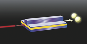
Quantum cryptography, quantum computing, and other futuristic technologies require pairs of photons that are entangled, meaning they share a quantum state. Now researchers reporting in Physical Review Letters have taken a step toward making those pairs as part of an integrated circuit for photons that could ultimately include tiny lasers and optical “wires.” The team used a semiconductor chip in a structure that could allow other components to be added, whereas previous chip-based devices weren’t as practical for such integration. Producing entangled pairs as part of such a chip is potentially a significant step toward making them commercially available and perhaps even leading to future quantum-optical gadgets.
To make entangled photon pairs, researchers typically hit a so-called nonlinear crystal with laser light. Some of the photons from the incoming beam convert into pairs of lower-energy photons that can then be used for encoding information and, in some cases, for carrying out rudimentary quantum computations. To integrate the components of such a photonic circuit into a single device, photonics experimenters have put many of the elements into chips of the semiconductor gallium arsenide, including laser sources and photonic waveguides, which are the optical equivalent of wiring. Some teams have recently produced photon pairs as well but not in a way that could easily work with an integrated circuit. For example, one device requires an insulating layer that would make electronic control difficult [1], while another requires the laser light to come in at an angle, out of the plane of the rest of the device [2].
Gregor Weihs of the University of Waterloo in Canada and the University of Innsbruck in Austria and his collaborators have now demonstrated a device that could be incorporated with other components on a single chip. “Our goal is to bake it all in one oven, so we have one cake,” says Waterloo team member Rolf Horn.
Gallium arsenide can generate lower-energy photons from laser light, but the conversion is inefficient unless the laser photons and the lower-energy photons travel at the same speed, meaning they are “phase matched.” (As in all solids, the speed of light in gallium arsenide depends on the wavelength.) “You need to get waves of different colors to be in phase with each other,” says Horn.
The problem was to phase match in a way that would not impede integration with other elements. The solution was a so-called Bragg-reflection waveguide, a structure developed by Amr Helmy and colleagues at the University of Toronto, and which the team has used in the past to guide light waves of a single wavelength. The device is reminiscent of a many-layer cake, with photons travelling through a layer in the middle whose height is near the wavelength of the laser (half a micron). The layers alternate between higher and lower values of the refraction index (determined by the amount of aluminum mixed in) and are tailored to allow one specific wavelength to survive in the central layer, thanks to vertical reflections and wave interference. The waveguide allows the lower-energy photons to remain in phase with the laser frequency. In addition, the structure separately stabilizes the laser photons with total internal reflection, the more conventional effect that keeps light traveling inside any fiber optic cable.
In trials, the device succeeded in producing a handful of photon pairs for every billion or so that were put in, an efficiency that approaches that of more conventional sources, Horn says. “This is an important step towards fully integrated quantum photonics devices,” says Jeremy O’Brien, who heads the Center for Quantum Photonics at the University of Bristol in England. “The authors have shown photon generation in an architecture that in principle allows direct electrical generation of photons [in the future],” O’Brien says, “in contrast to typical schemes [today] that require a laser to generate the photons.”
The team now plans to combine their photon-pair source with features that would manipulate the photons into having correlated polarizations—the type of entanglement most often used for quantum information. For fully integrated photonic chips, however, one component is still missing: single-photon detectors that can turn the optical information into an electronic signal. One option would be to use superconductors, Horn says, a technique that was recently demonstrated by another team [3].
–Davide Castelvecchi
Davide Castelvecchi is a freelance science writer in Rome.
References
- A. Orieux, X. Caillet, A. A. Lemaître, P. Filloux, I. Favero, G. Leo, and S. Ducci, “Efficient parametric generation of counterpropagating two-photon states,” J. Opt. Soc. Am. B 28,45 (2010)
- M. Ravaro, L. Lanco, X. Marcadet, S. Ducci, V. Berger, and G. Leo, “Parametric fluorescence in semiconductor waveguides,” C. R. Phys. 8,1184 (2007)
- W. Pernice, C. Schuck, O. Minaeva, M. Li, G. N. Goltsman, A. V. Sergienko, and H. X. Tang, “High Speed and High Efficiency Traveling Wave Single-Photon Detectors Embedded in Nanophotonic Circuits,” arxiv:1108.5299


