What Are the Resolution Limits in Electron Microscopes?
The last decade has seen unprecedented strides to ever-improving resolutions in electron microscopes. To focus the electrons, these microscopes use round electro-magnetic lenses that, unlike glass lenses in optical microscopes, have a positive spherical aberration [1]. Because of this electrons traveling at larger angles away from the incident beam direction are focused more strongly than those traveling at smaller angles, blurring the image. While the wavelength of the electrons used is very small, typically in the range 0.02-0.037 angstroms, for many years it was impossible to come close to the theoretical wavelength-limited resolution because of the finite spherical aberration. A commonly used analogy is that taking images with imperfect electron microscope lenses is like trying to see through glass milk bottles.
It has been known for many years that the way to create negative spherical aberration magnetic lenses is to break the symmetry and use multipole lenses [1]; with round lenses the magnetic field lines are largely parallel to the electron beam direction, whereas in multipole lenses they are perpendicular to it. However, this involves controlling a very large number of different lens elements at the same time, which proved difficult until computer control was introduced (e.g., Refs. [2,3]). Not too long after this, designs to correct the next large problem, chromatic aberration (focal length dependent on wavelength) appeared and were quickly implemented in commercial machines [4].
It looked like electron microscopes were on the path to ever-increasing resolution, with no foreseeable barriers to ever-better performance. Alas, it appears this was too optimistic. In Physical Review Letters, Stephan Uhlemann and colleagues at Corrected Electron Optical Systems GmbH (CEOS), Germany, report an unexpected limit to resolution [5], namely, magnetic noise caused by thermal activation of currents or spins in the metal components. Due to the longer optical path that they travel in aberration-corrected instruments, the electrons are sensitive to very small magnetic fields, which the authors estimate to be of the order of 0.1 nanotesla, about a hundred thousand times smaller than the Earth’s magnetic field.
The experiments performed by Stephan Uhlemann and co-workers involved modifying an electron microscope by removing the aberration corrector and replacing it with a tube which could be cooled, and then putting different tubes within it (a stainless steel and a permalloy material were used). They then examined how the resolution depended upon both the inner tube material as well as the temperature, showing a significant improvement at lower temperatures which is consistent with thermal magnetic noise.
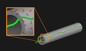
Any transmission electron microscope contains many metal parts. Most of these parts are structural but others carry current for lenses, are involved in transmission of magnetic fields, or are part of apertures used to select which parts of the electron beam are involved in the final image or spectra. Often these are inhomogeneous alloys containing precipitates, dislocations, grain boundaries, and other phases chosen to improve mechanical and electrical performance or simply cost. At any given instance of time there can be local fluctuations in electrical currents/spins (what is called Johnson-Nyquist noise [6,7]), as illustrated in Fig. 1, which lead to fluctuating magnetic fields in sensitive magnetic devices such as SQUIDS.
While the time-averaged effect of these fields is small, the swift electrons in the microscope are traveling at about half the speed of light and so can be deflected by the instantaneous magnetic fields. Time averaged over the many electrons that make up the final image (typically 103– 105 are detected in any single pixel of a CCD camera), this reduces the coherence of the electron beam and consequently the resolution. The authors estimate that the resulting resolution limit is in the range 0.5– 0.8Å, which is consistent with the best that has been achieved to date.
Of course, improving the resolution to (for instance) 0.1Å is a noble goal, but, by itself, the utility of doing this is unclear considering the ever-increasing cost of transmission electron microscopes, which is now approaching ten million dollars. Unless the focus is on exceedingly thin and relatively simple samples such as single graphene sheets, improving the resolution of the microscope may make the images crisper, but it has drawbacks. The sampling theorem is inescapable, requiring the effective distance between pixels in the image to be four or more times smaller than the resolution, so every factor of 2 resolution improvement requires a factor of 4 higher electron flux/dose and therefore more beam damage. At higher resolutions, nonlinear imaging contributions as well as the ever-present multiple or dynamical diffraction of electrons and inelastic scattering effects do not vanish. For instance, despite the relatively high voltages used, even a single atom of gold scatters the electrons many times. As a consequence one always has to be wary of oversimplified interpretations, even with the most advanced microscopes. To date, nobody has been able to construct a “dynamical-diffraction corrector,” and the most important corrector of all, the “user interpretation corrector” is not in sight.
In many ways, the real payoff of improved performance of the microscope is better signal-to-noise; improving the resolution from (for instance) 0.8Å to 0.4Å improves the ability to detect features by a factor of 2. Indeed, many of the recent achievements of aberration-corrected microscopes can be attributed to much better signal-to-noise.
So, where do we go next? One approach would be to reduce the distance over which the electrons are exposed to the magnetic noise by increasing the strength of the field to get the same lensing effect. Another would be to try and find different materials for pole pieces and liner tubes; there are roughly a hundred different stainless steels, all with slightly different properties, and cost-wise, highly pure single crystals are not unreasonable. (These are routinely used for aircraft turbine blades, so it can be done.) Of course one can reduce the temperature of the whole instrument to that of liquid helium, but beyond a demonstration experiment this is not likely to be practical, certainly not in a routine laboratory environment.
Now we wait and see what develops. It is certainly premature to claim that electron microscopes are approaching any fundamental limit; this is far from the case. More realistically we are going to see a slow down in the rate of improvement as solutions to the fundamental engineering problems of designing the electron optics to reduce noise sensitivity is attacked.
References
- O. Scherzer, “Das theoretisch erreichbare Auflösungsvermögen des Elektronenmikroskops,” Z. Physik 114, 427 (1939)
- M. Haider, H. Rose, S. Uhlemann, B. Kabius, and K. Urban, “Towards 0.1 nm Resolution with the First Spherically Corrected Transmission Electron Microscope,” J. Electron Microsc. 47, 395 (1998)
- O. L. Krivanek, N. Dellby, A. J. Spence, R. A. Camps, and L. M. Brown, in Electron Microscopy and Analysis 1997, edited by J. M. Rodenburg, Proceedings of the Institute of Physics Electron Microscopy and Analysis Group Conference (IOP, Bristol, 1997)[Amazon][WorldCat]
- M. Haider, P. Hartel, H. Muller, S. Uhlemann, and J. Zach, “Information Transfer in a TEM Corrected for Spherical and Chromatic Aberration,” Microsc. Microanal. 16, 393 (2010)
- S. Uhlemann, H. Müller, P. Hartel, J. Zach, and M. Haider, “Thermal Magnetic Field Noise Limits Resolution in Transmission Electron Microscopy,” Phys. Rev. Lett. 111, 046101 (2013)
- J. B. Johnson, “Thermal Agitation of Electricity in Conductors,” Phys. Rev. 32, 97 (1928)
- H. Nyquist, “Thermal Agitation of Electric Charge in Conductors,” Phys. Rev. 32, 110 (1928)


