Single Spins Charge Ahead
In nanoscale devices like a quantum dot, the presence of even a single excess electron can change the material’s electrical or optical properties. Similarly, the charge on biological macromolecules, such as DNA, affects their interactions with other molecules. Researchers are therefore searching for new ways to sense localized charges on materials in a variety of environments. In Physical Review Letters, Jörg Wrachtrup at the University of Stuttgart, Germany, and his collaborators report a prototype electrometer consisting of an atom-sized defect in diamond, called a nitrogen-vacancy center ( ), that is capable of sensing a single charge on a nearby nitrogen-vacancy center. The electrometer could, in principle, work at room temperature and atmospheric pressure and requires no electrical contact with the sample [1]. The technique builds on the group’s earlier work, in which they established that the resonant frequency of a ’s spin precessing in a magnetic field is influenced by an applied electric field [2]. They now show that this spin resonance signal is sensitive enough to detect the electric field from a single electron nanometers ( ) away.
Several methods for sensing individual charges already exist. For example, electrostatic force microscopy [3] and scanning single-electron transistor microscopy [4] have provided astonishing nanoscale views of the distribution of charge states in ceramics and semiconductor devices. A new sensor based on spin resonance is an appealing complement because it requires no electrical connection to the sample, can operate under ambient conditions, and can potentially tolerate environments, such as liquids or harsh chemicals, that are inhospitable to other techniques. In fact, center spins have already been pressed into service as nanoscale magnetic-field sensors that can detect a single spin [5]. They can also function as sensitive thermometers [6] that work inside living cells [7].
The center is a point defect in diamond that consists of a missing carbon atom (a vacancy) and a nitrogen atom that substitutes for a carbon atom on an adjacent lattice site. At the defect site, the dangling bonds of the surrounding atoms hybridize and form localized electronic energy levels similar to those of a molecule. When an center is negatively charged (denoted ), it has a total electronic spin of , giving it three possible spin projections ( , , ). An exciting property of is that after being optically excited to a higher-energy electronic state, its relaxation back to the lowest energy state depends on its spin projection. If the spin projection is , it almost always relaxes by emitting a photon. Relaxation for the other two spin projections ( ) could either involve emission of a photon, or it could involve a long-lived intermediate state, with no visible photon emission. As a result, the intensity of light emitted by the depends on its electronic spin projection, which in turn provides an optical method to detect the changes in the average spin projection that occur in a spin resonance experiment. This property, along with the atom-scale size of the defects and their naturally narrow spin resonance linewidths, makes centers attractive as optically addressed nanoscale sensors that use spin resonance to monitor the local environment.
In 2011, Wrachtrup and his group showed that a center’s spin resonance depends on local electric field [2]. In simple terms, this dependence exists because a nearby electric field changes the symmetry of the nitrogen-vacancy center. When no electric field is present, the four dangling bonds around the vacancy have roughly the shape of a camera tripod (three bonds form the legs and one bond forms the pole supporting the camera). But in an electric field, the tripod becomes slightly distorted. As a result, the nitrogen-vacancy center’s electron density and spin energies shift, which the researchers can detect as a shift in the spin resonance frequency.
The researchers have now shown that the vacancy is sufficiently sensitive that it can detect the electric field of a single charge. To demonstrate this level of sensitivity, Wrachtrup and co-workers first needed a way to control a localized electron in the vicinity of the defect. They take advantage of the fact that, like many semiconductor defects with deep energy levels, centers can be stable in more than one charge state. In particular, they can be negatively charged with one electron ( ) or electrically neutral ( ). In an earlier paper [8], the Stuttgart group provided evidence that the charge state could be optically controlled with a red laser.
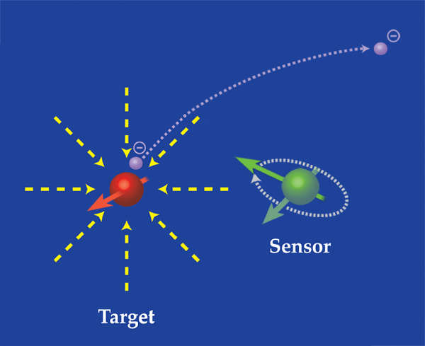
In this new work, Wrachtrup combines these two capabilities—electric-field detection and optically induced charging—in a pair of nearby centers. They designate one center as the electrometer (the “sensor”) and the other as a controllable source of a single electron charge (the “target,” see Fig. 1). These two centers are spaced about apart within a single crystal of diamond. The two defects have a different orientation with respect to the diamond crystalline axes, which allows their spin resonance signals to be studied independently. The researchers measure the magnetic resonance signal of the sensor using spin resonance protocols that maximize the sensitivity of the spin precession frequency to local electric fields. When they take a Fourier transform of this data, they observe two distinguishable resonant features: One feature corresponds with the target in the state and the other with the target in the state. The amplitude of each of these features corresponds to the relative amount of time the target spent in each charge state, proving the sensor’s sensitivity to the presence of a single, nearby charge. This direct sensitivity to charge allows them to confirm their earlier conclusion [8] that increasing red illumination increases the probability of the target being .
The real advance, however, is the demonstration that the spin state of a single diamond center is sensitive to the electric field from a single, localized charge. It is easy to imagine extending their experiment by scanning the sensor relative to a target in a different material to build up an image of the local charge environment. Since a scanning field sensor could operate under a wide range of conditions, including in a liquid, the device would extend the choices for fundamental charge sensing in nanoscience and potentially biology, where electrostatics play a crucial role [9].
Like many ideas in nanoscience, moving from a proof-of-concept demonstration to a useful tool is a major challenge. Among the obstacles is the low flux of photons emitted from a single center, which will potentially require long data collection times. Additionally, the present experiment was conducted using well-controlled centers located deep within a single crystal of diamond. In contrast, a useful scanning sensor would need an NV center placed a few nanometers from the surface or embedded within a tiny nanostructure. Such surface proximity tends to shorten the spin coherence time relative to “deep” centers, which correspondingly decreases the sensitivity even for perfect diamond crystals [10]. Fortunately, the electric-field sensing protocol is fairly insensitive to magnetic-field noise, providing some isolation from decohering surface spins. Also, several groups are working to overcome similar issues in spin sensors that use centers. Even if substantial effort lies ahead, this work is an important step forward for nanoscale sensing of fundamental charges.
References
- Florian Dolde et al., “Nanoscale Detection of a Single Fundamental Charge in Ambient Conditions Using the Center in Diamond,” Phys. Rev. Lett. 112, 097603 (2014)
- F. Dolde et al., “Electric-Field Sensing Using Single Diamond Spins,” Nature Phys. 7, 459 (2011)
- C. Schönenberger and S. F. Alvarado, “Observation of Single Charge Carriers by Force Microscopy,” Phys. Rev. Lett. 65, 3162 (1990)
- M. J. Yoo, T. A. Fulton, H. F. Hess, R. L. Willett, L. N. Dunkleberger, R. J. Chichester, L. N. Pfeiffer, and K. W. West, “Scanning Single-Electron Transistor Microscopy: Imaging Individual Charges,” Science 276, 579 (1997)
- M. S. Grinolds, S. Hong, P. Maletinsky, L. Luan, M. D. Lukin, R. L. Walsworth, and A. Yacoby, “Nanoscale Magnetic Imaging of a Single Electron Spin Under Ambient Conditions,” Nature Phys. 9, 215 (2013)
- D. M. Toyli, C. F. de las Casas, D. J. Christle, V. V. Dobrovitski, and D. D. Awschalom, “Fluorescence Thermometry Enhanced by the Quantum Coherence of Single Spins in Diamond,” Proc. Natl. Acad. Sci. U.S.A. 110, 8417 (2013)
- G. Kucsko, P. C. Maurer, N. Y. Yao, M. Kubo, H. J. Noh, P. K. Lo, H. Park, and M. D. Lukin, “Nanometre-Scale Thermometry in a Living Cell,” Nature 500, 54 (2013)
- G. Waldherr, J. Beck, M. Steiner, P. Neumann, A. Gali, T. Frauenheim, F. Jelezko, and J. Wrachtrup, “Dark States of Single-Vacancy Centers in Diamond Unraveled by Single Shot NMR,” Phys. Rev. Lett. 106, 157601 (2011)
- B. Honig and A. Nicholls, “Classical Electrostatics in Biology and Chemistry,” Science 268, 1144 (1995)
- K. Ohno, F. Joseph Heremans, L. C. Bassett, B. A. Myers, D. M. Toyli, A. C. Bleszynski Jayich, C. J. Palmstrm, and D. D. Awschalom, “Engineering Shallow Spins in Diamond with Nitrogen Delta-Doping,” Appl. Phys. Lett. 101, 082413 (2012)