Landmarks—Accidental Discovery Leads to Calibration Standard
Landmarks articles feature important papers from the archives of the Physical Review journals.
The classical Hall effect describes the deflection of electric current in a magnetic field. The 1980 discovery of the quantum version was a surprise whose theoretical basis still contains some puzzles. Its practical significance, however, was immediately obvious, and today the quantum Hall effect, recognized in the 1985 Nobel Prize in physics, is the basis of the standard definition of the unit of electrical resistance, the ohm.
In the Hall effect, electrons passing through a conducting strip are deflected sideways by a perpendicular magnetic field. The density of charge carriers becomes greater on one side than the other, creating an electric potential that is measurable as the Hall voltage, at right angles to the current. In quantum-mechanical terms, however, thinking of an electric current as a simple flow of electrons is highly misleading, and the route that led to the discovery of the quantum Hall effect started from very different considerations.
In 1930, the Russian theorist Lev Landau analyzed the behavior of a two-dimensional gas of electrons. In a sufficiently strong perpendicular magnetic field, the electrons could only move, Landau realized, in circular paths. Moreover, these orbits—Landau levels—would be quantized, like the orbitals in the hydrogen atom, because the wavelike electron could only execute an orbit if the circumference were equal to an integer number of wavelengths.
The 1959 invention of the MOSFET (metal-oxide-semiconductor field-effect transistor) allowed physicists to study electron behavior in a nearly ideal 2D gas. In a MOSFET, conduction electrons travel in a thin surface layer, and a “gate” voltage controls the number of charge carriers in this layer. To explore quantum effects, researchers needed to operate high-purity MOSFETs at liquid-helium temperatures.
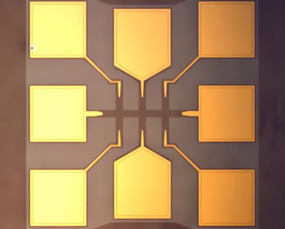
In 1980, Klaus von Klitzing of the University of Würzburg, Germany, was conducting experiments at the Max Planck High Magnetic Field Laboratory in Grenoble, France, using high-quality MOSFETs built by his colleagues specifically for Hall voltage measurements. Other experimenters, von Klitzing says, had noticed anomalies in the resistance of semiconductors in strong magnetic fields, but no one had looked for a Hall voltage. He found that as the MOSFET gate voltage increased (which increased the number of conduction electrons), the Hall voltage decreased smoothly—except that at three places, it stayed constant for a while, creating a step or plateau in the voltage curve.
Von Klitzing explained this unexpected behavior by combining classical and quantum ideas. Classically, the Hall voltage drops as the number of charge carriers increases (for fixed current). Quantum mechanically, each added electron enters its own Landau level (circular orbit) at a different location, and there are many available with the same energy. But the area of the sample limits the number of these orbits. Once they are all filled, there is no available quantum state for a new electron unless it has enough energy to fill a higher-energy Landau level. The gate voltage must be raised until the newly created conduction electrons have enough energy to start filling this next level. In the meantime, the Hall voltage remains constant to high precision, since not a single electron can enter or leave the conducting population.
At the plateaus, von Klitzing realized, the Hall voltage becomes equal to a combination of fundamental physical constants (the charge of the electron and Planck’s constant) multiplied by an integer corresponding to the quantized energy of the filled Landau levels. In short, the Hall voltage is quantized.
It was 10 or 15 years before theorists came up with a better understanding of the quantum Hall effect, says JT Janssen of the UK National Physical Laboratory in Teddington. The modern view is that the interior of the device is an insulator because electrons are trapped in Landau levels that do not move. Current travels only around the edges, where the Landau levels form a chain of connected semicircles. The quantization rule that von Klitzing derived nevertheless holds true, although Janssen says that even now, no theory fully explains why the quantization is so perfect, unaffected by the geometry and purity of the material.
Von Klitzing says that the title and abstract of his original manuscript pointed out the utility of the quantum Hall effect for resistance calibrations, but the referees objected. Since then, however, the effect has been widely adopted as a basis for defining the ohm. Resistance standards based on the quantum Hall effect in graphene, the truly two-dimensional carbon sheet molecule, now exist. So, von Klitzing says, the original title, “Realization of a Resistance Standard Based on Natural Constants,” is finally correct.
This research is published in Physical Review Letters.
–David Lindley
David Lindley is a freelance science writer, now retired. His most recent book is The Dream Universe: How Fundamental Physics Lost Its Way (Penguin Random House, 2020).
More Information
Nobel Focus: Current for a Small Charge (Focus story on the fractional Quantum Hall effect)
Klaus von Klitzing, “25 Years of Quantum Hall Effect (QHE),” Séminaire Poincaré 2, 1 (2004) free pdf
von Klitzing Nobel Prize from the Nobel Foundation


