Intramolecular Imaging at Room Temperature
The year of 1955 saw the first observation of individual atoms [1]. German physicist Erwin Wilhelm Müller and his student Kanwar Bahadur, from Pennsylvania State University, used a field ion microscope to image the atoms at the apex of a sharp tungsten needle held at liquid-nitrogen temperature. The real breakthrough in atom imaging, however, came more than 25 years later, with the invention of the scanning tunneling microscope in 1981 [2] and the related atomic force microscope in 1986 [3]. The development of these imaging devices has revolutionized our ability to study surfaces at the atomic level. Imaging single atoms adsorbed on solid surfaces using such microscopes is today a common practice. However, resolving the internal structure of an adsorbed molecule at room temperature has remained a challenge—until now. In a new study, Franz Giessibl from the University of Regensburg in Germany and colleagues [4] describe an approach that provides intramolecular and intermolecular imaging of adsorbed molecules at room temperature.
In scanning tunneling microscopy (STM), a sharp tip is brought close to the substrate to be imaged. The tip is mounted on a piezoelectric device that controls the tip position and scans it over the substrate surface. The distance between the substrate and tip is so small (about 1 nanometer) that, when a bias voltage is applied between the tip and substrate, electrons can quantum-mechanically tunnel from the substrate to the tip or vice versa through the empty gap that separates them. The resulting tunneling current, which is a function of the applied bias, tip position, and the density of electronic states near the Fermi level, is measured and displayed as an image. The image contains information about the structural and electronic properties of the substrate surface. However, STM cannot, in principle, resolve the intramolecular structure of molecules adsorbed on solid surfaces. This is because the technique is not sensitive to the electronic states near the core of the sample atoms—states that are far from the Fermi level. Such information would provide a “fingerprint” to identify the atoms that make up the molecules.
However, in 2008 researchers [5] managed to circumvent this limitation and obtain intramolecular resolution by trapping molecular hydrogen between the substrate and the apex of the tip. One year later, such resolution was also attained [6] by decorating the tip of an atomic force microscope with a single carbon monoxide molecule. Nevertheless, these techniques have several drawbacks. First, they involve modifying the standard imaging setup: in the first case, adding molecular hydrogen to the tunneling gap, and in the second, tailoring the tip. Second, cryogenic temperatures are required to keep these specially engineered tunneling junctions stable. Third, the methods require data acquisition times of the order of tens of seconds to produce the images. These long acquisition times make the techniques susceptible to thermal drift—unwanted motion of the tip caused by temperature gradients. Thermal drift is one of the reasons why these approaches have only been performed at cryogenic temperatures.
In their study, Giessibl and colleagues used a known trick that allows these types of experiments to be made at room temperature, substantially reduces the acquisition time, and doesn’t require specially engineered junctions. The tunneling gap that the electrons encounter when tunneling from substrate to tip (or vice versa) can, at least for small applied bias voltages, be approximated by a rectangular potential barrier. The height of this barrier is very sensitive to small variations of the electrical dipole of the adsorbed molecule. To measure these variations, the authors modulated the width of the tunneling gap by applying a small sinusoidal voltage to the piezoelectric device. This modulation generates a sinusoidal variation of the tunneling current. Using an electronic device known as a lock-in amplifier, the researchers then measured the derivative of the current with respect to the gap width. This signal depends on the barrier height, hence measuring it provides information about the molecule’s dipole.
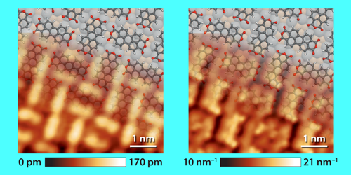
If the frequency of the sinusoidal voltage is appropriately tuned, one can simultaneously record a standard (constant-current) STM image as well as a spatial map of the barrier height. This approach has been pursued in the past [7–10], but the spatial resolution obtained so far has been insufficient to resolve the internal structure of a molecule. Giessibl and colleagues substantially improve the method by properly taking into account the sinusoidal voltage modulation and the behavior of the electronic module that converts the tunneling current into a voltage. A comparison of the STM image with the spatial map of the barrier height shows a large difference in spatial resolution between the image and the map (Fig. 1). In the STM image, the adsorbed molecule, a PTCDA (perylene-3,4,9,10-tetracarboxylic dianhydride) molecule, appears as two-lobed features (the lobes can be associated with the perylene core of the PTCDA molecule), whereas the spatial map of the barrier height reveals the internal structure of the molecule.
The authors expect that the method will play a pivotal role in high-resolution imaging of molecules at room temperature. Knowledge of the intramolecular structure of individual molecules is crucial for several research areas, including molecular electronics—a field of nanotechnology that uses molecular building blocks comprising one or a few molecules to build electronic devices. To achieve such imaging, however, researchers will need to investigate issues such as the dependence of the intramolecular and intermolecular structure on the applied bias between substrate and tip.
This research is published in Physical Review Letters.
References
- E.W. Müller and K. Bahadur, “Field Ionization of Gases at a Metal Surface and the Resolution of the Field Ion Microscope,” Phys. Rev. 102, 624 (1956) .
- G. Binnig and H. Rohrer, “Scanning Tunneling Microscopy,” Helv. Phys. Acta 55, 726 (1982).
- G. Binnig, C.F. Quate, and C. Gerber, “Atomic Force Microscope,” Phys. Rev. Lett. 56, 930 (1986) .
- F. Huber, S. Matencio, A. J. Weymouth, C. Ocal, E. Barrena, and F. J. Giessibl, “Intramolecular Force Contrast and Dynamic Current-Distance Measurements at Room Temperature,” Phys. Rev. Lett 115, 066101 (2015).
- R. Temirov, S. Soubatch, O. Neucheva, A.C. Lassise, and F.S. Tautz, “A Novel Method Achieving Ultra-High Geometrical Resolution in Scanning Tunnelling Microscopy,” New. J. Phys 10, 053012 (2008) .
- L. Gross, F. Mohn, N. Moll, P. Liljeroth, and G. Meyer, “The Chemical Structure of a Molecule Resolved by Atomic Force Microscopy,” Science 325, 1110 (2009) .
- G. Binnig, H. Rohrer, C. Gerber, and E. Weibel, “Surface Studies by Scanning Tunneling Microscopy,” Phys. Rev. Lett. 49, 57 (1982) .
- J. A. Stroscio, R. M. Feenstra, and A. P. Fein, “Electronic Structure of the Si(111) Surface by Scanning Tunneling Microscopy,” Phys. Rev. Lett. 57, 2579 (1986) ; R. M. Feenstra, J. A. Stroscio, and A. P. Fein, “Tunneling Spectroscopy of the Si(111) Surface,” Surf. Sci. 181, 181 (1987) .
- R. J. de Vries, A. Saedi, D. Kockmann, A. van Houselt, B. Poelsema, and H. J. W. Zandvliet, “Spatial Mapping of the Inverse Decay Length Using Scanning Tunnelling Microscopy,” Appl. Phys. Lett. 92, 174101 (2008) .
- L. Vitali, G. Levita, R. Ohmann, A. Comisso, A. De Vita, and K. Kern, “Portrait of the Potential Barrier At Metal-Organic Nanocontacts,” Nature Mater. 9, 320 (2010) .


