Tiny Digital Bits in Ferroelectric Material
As electronic devices shrink, the need to store more information in smaller spaces increases. Researchers have now shown that a single digital bit—a 0 or 1—can be stored in an area roughly 5 nanometers on a side using the persistent patterns of electric fields in a so-called ferroelectric material. The team says that the results could ultimately lead to devices storing 100 times as much information in a given area as is possible in commercial devices today, but they also acknowledge that significant technological challenges stand in the way of such an achievement. If digital memories don’t turn out to be practical, the new technique also allows a new level of precision in experiments with ferroelectric materials.
In a ferroelectric material, electrically charged ions naturally segregate to create persisting internal electric fields known as polarization. The polarization in such materials takes on a single direction across a region—from a few nanometers to several millimeters across—known as a domain but can vary from one domain to another. The polarization prevailing in any domain can be altered by applying an external electric field. So ferroelectrics can store digital information encoded in the up-or-down direction of the polarizations of a sequence of domains, which act as digital bits.
The methods used previously to manipulate these ferroelectric patterns relied on placing a highly charged, sharp metallic tip in contact with the surface, to create the strong, reorienting electric field. However, the physical contact often damaged the ferroelectric material or the metallic tip, degrading performance over time.
Now Xiaozhou Liao and colleagues from the University of Sydney in Australia have demonstrated that these problems can be avoided by using an electron beam flowing from a metal tip that never contacts the material directly. Their technique also makes it possible to manipulate the pattern with fine resolution, with one bit occupying a zone only 5 nanometers on a side, compared with 50 nanometers for commercial devices.
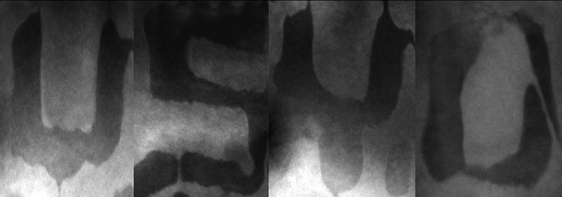
The team demonstrated the method in experiments with the ferroelectric material hexagonal yttrium manganite . In a thin sample of this crystal, the polarization takes one of two possible values that point in opposite directions within the plane. First, Liao and colleagues used a transmission electron microscope to measure and map the polarization pattern over a set of ferroelectric domains. Then they used the microscope’s 200-nanometer-wide electron beam at higher energy to illuminate a portion of one domain. They found that the electrons, in passing through the material, created an electric field pointing radially outward, from the beam center toward its edges. The field was strong enough to reverse the polarization direction within part of the beam on the side where the field was opposite to the polarization.
The researchers also showed that the resulting change—which could be used to store one bit of information—remained stable for one month afterward. Experiments also showed that the induced change could be undone by illuminating the area again, with the beam shifted laterally in order to apply the opposite electric field.
As Liao admits, he and his colleagues are not entirely sure how the electron beam works its effect. A buildup of negative electric charge from the beam on the material surface would produce a field pointing inward, the opposite of what they observed. Rather, they believe, the strong field pointing outward comes from the accumulation of positive charges created by the passing beam.
Liao suggests that this technique could lead to information storage at densities 100 times higher than today’s memories. But he also cautions that significant further development would be needed, especially in miniaturizing electron beam sources.
Another problem is the material’s domain structure, says Takao Matsumoto of the University of Tokyo. “You can create a single switched domain, as this study shows, yet it's unclear if that domain would stay unchanged after [switching] another domain nearby.”
But even if high density memories can’t be produced, Liao and colleagues believe their electron-beam-controlled domain switching technique will be useful in the study of ferroelectric materials. For example, they would like to better understand the factors that affect domain switching, such as boundaries and crystal defects, since these materials have other uses in the electronics industry
This research is published in Physical Review Letters.
–Mark Buchanan
Mark Buchanan is a freelance science writer who splits his time between Abergavenny, UK, and Notre Dame de Courson, France.