Graphene’s prisoners
Like semiconductor alloys that are amenable to band-gap engineering, graphene is more customizable from a technological perspective when slightly contaminated with defects and disorder. In its pure form, graphene’s energy spectrum does not have the band gap needed to control the transport characteristics of a device. Controlled addition of defects can change the properties of graphene to allow for new applications.
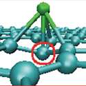
Writing in Physical Review Letters, Ovidiu Cretu and co-workers at the University of Strasbourg, France, together with collaborators at the Universities of Helsinki and Aalto, both in Finland, produce defects on a graphene surface by electron irradiation and subsequent annealing. Then, using transmission electron microscopy and density-functional calculations, they show that tungsten atoms, evaporated onto the surface from a heated filament, become trapped and localized by strain fields around the defects. The tungsten atoms can be made to migrate to less pristine regions of the hexagonal graphene lattice. These migrating metal atoms may enable more controlled engineering of electronic and magnetic structure of graphene than that offered by substitutional doping. – Sami Mitra