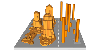
Steps Towards Slimmer Nanorods
Arrays of thin noble-metal nanorods have enormous potential for catalysis as well as other applications where a large surface-to-volume ratio is desired. However, one particularly crucial unknown is the minimum diameter nanorod achievable by physical vapor deposition (PVD), a versatile method for fabricating nanostructures from essentially any material. So far, diameters down to nanometers (nm) have been reached with PVD, but experimentalists would benefit from having a clear minimum-diameter target in sight. Now, writing in Physical Review Letters, Xiaobin Niu and colleagues from the University of Connecticut, Storrs, present a model and experiments that show this minimum size could be much smaller than previously thought.
Solid films grown by PVD are usually fabricated one layer of atoms at a time, but to grow nanostructures, one has to build up multiple partial or incomplete layers on the substrate. Theoretical models of this process haven’t taken into account multilayered surface steps in the early growth phase because they were thought to be too kinetically unstable to have an effect on the final structure. In their model, Niu et al. show that these surface steps are, in fact, important because they dictate how the next layer of adatoms will position themselves. They find that growth conditions favoring multilayered surface steps over monolayer steps are the key to growing small, well-separated nanorods.
Optimizing for growth conditions like the choice of substrate, substrate temperature, and the rate and angle of deposition, Niu et al. show that well-separated nanorods with diameters of for copper and nanometers for gold should be possible, a prediction they verify with simulations and electron micrographs of actual nanorods they prepared in the lab. – Daniel Ucko


