Racking up the electron billiards
The confinement of electrons to regions so small that quantum effects are observed is compelling for applications in quantum computing, microchip fabrication, and nanoscale laser fabrication. Such nanostructures are typically studied with scanning probes like STM (scanning tunneling microscopy) or AFM (atomic force microscopy). Reporting in Physical Review Letters, Guillaume Schull, Michael Becker, and Richard Berndt of the University of Kiel have now combined the spectroscopic utility of optical probes with the atomic resolution of STM to create detailed images of electrons corralled into nanoscale metal islands on a gold surface.
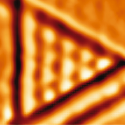
The researchers used tungsten tips to scan a chemically etched gold surface and collected photons excited by the tunneling current at the junction between the tip and the metal. The light, which was produced by the collective electron oscillations in the metal, called plasmons, was routed through an optical fiber to a spectrometer to create maps of photon energy as a function of position on the surface. These maps show striking variations caused by standing electron waves on the surface structures. In one case, the authors scanned over a triangular metal island and saw undulations in the electron density of states caused by quantum interference effects.
In addition to the spatial map of quantum confinement, the spectral data show evidence of inelastic tunneling between the tip and the two-dimensional electron gas at the surface. This ability to examine the detailed physics of plasmonic photon generation at the atomic scale should be valuable in probing the optical properties of electrons confined to nanostructures. – David Voss


