A Graphene Waveguide For Electrons
A waveguide can steer single photons along a well-defined path, but creating the equivalent for electrons has proved tricky. Now researchers have demonstrated a potentially high-fidelity waveguide that transports single electrons in a 2D material. They used a carbon nanotube to mark out a narrow track for electrons to move across graphene, a single-atom-thick material. The device design could work in large circuit networks and could enable scientists to create new templates for quantum computing processors that use information stored in the quantum states of electrons.
In many cases, a waveguide can support several different modes, or wave patterns, for a wave traveling through it, just as a vibrating string or drumhead has various vibration patterns. An electron carrying information in its quantum state and acting according to its wave nature can travel though a waveguide, but if multiple modes are available, then the electron can switch between them and lose information. So a key property for an electron waveguide is that it should host just one wave mode of the electron. A second key property is that the electron’s velocity should be independent of its energy. This so-called “linear dispersion” property prevents distortion of the electron waveform.
Waveguides exist that can steer electrons through a 2D material, but at best they achieve only few-mode guiding, and their dispersion properties are not linear. Current devices also exhibit poor guiding efficiency, with electrons leaking out of the waveguide into the surrounding material, says Jean-Damien Pillet from the Paris Polytechnic Institute. The new device that he and his colleagues have built solves these problems.
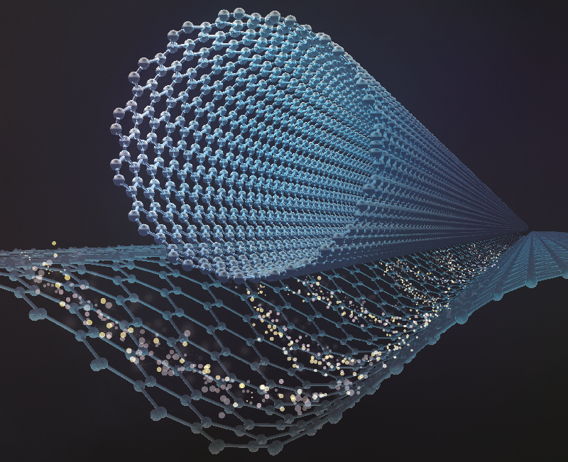
The team’s device includes a graphene flake—a single atomic layer of carbon—sandwiched between two insulating sheets. On top of this structure sits a single carbon nanotube (CNT). A voltage applied across the CNT induces an electrostatic potential shaped like a rain gutter that extends down into the flake. The potential traps the graphene’s electrons directly beneath the CNT and restricts them to move only along the length of the channel, which is about 500 nanometers long. The electrons thus behave as if they are in a physical waveguide.
The team did not require additional technology to monitor the electrons in the waveguide, Pillet says. When electrons in the underlying graphene flake switch from unconstrained to waveguide-directed motion, the nanotube’s charge changes in a very predictable way. By monitoring these changes at a temperature of 1.6 K, the team could precisely deduce the behavior of the waveguide’s electrons.
To check their design, the team varied the width and depth of the guide’s channel by varying the width and position of the CNT and by changing the applied voltage. When the width was narrow enough, the team could tune the depth to achieve single-mode guiding of the electrons.
This experiment is the first demonstration of a single-mode electron waveguide in a 2D material, says condensed matter physicist Marc Bockrath of Ohio State University in Columbus. David Goldhaber-Gordon, of Stanford University, California, who studies electrons confined in submicrometer structures, calls the device “clever and well-implemented,” especially because of its built-in measurement technique. He says that confining electrons in a waveguide is tricky because of the narrow electrostatic potential needed for the channel, but the team solved this problem by using a CNT.
Stephan Roche at the Catalan Institute of Nanoscience and Nanotechnology in Spain concurs, saying that the key to the result is the researchers’ choice of materials. The electrical interactions between the materials are weak enough that they don’t damage each material’s electronic properties but strong enough to allow for the long-range transfer of the guiding potential from the CNT to the graphene, he explains.
Pillet says that this waveguide design could provide a platform for controlled transmission of quantum information using electrons. It could also support compact optics-like experiments with electrons, allowing the production of sensitive electron interferometers that are a fraction of the size of those currently used for photons. Other applications include ultrafast switches and reconfigurable circuits. But for any of these technologies to become practical, the waveguides would need to operate at room temperature and transmit electrons over longer, micrometer-scale distances, says Goldhaber-Gordon.
This research is published in Physical Review Letters.
–Katherine Wright
Katherine Wright is the Deputy Editor of Physics Magazine.


