Harnessing Bound Charge in Semiconductors
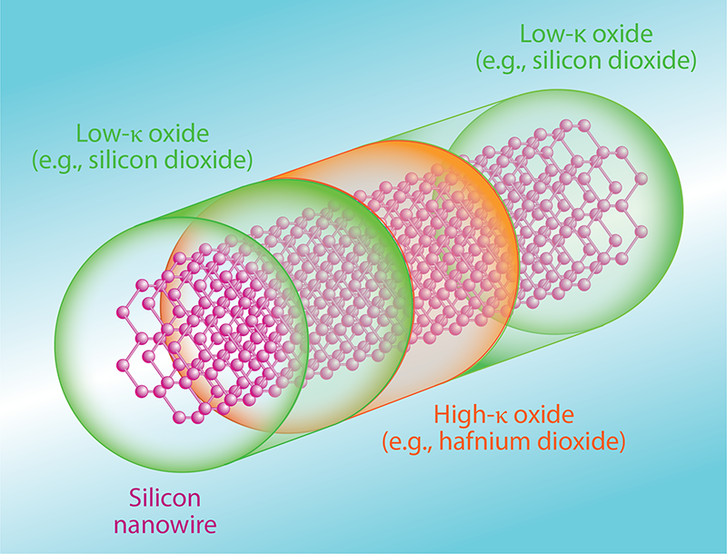
For transistors that rely on quantum tunneling between materials, performance depends on how readily charge can tunnel across the material junctions. Now, Raphaël Prentki of McGill University in Canada and colleagues have proposed a way to create sharper, more traversable junctions in these so-called tunnel field-effect transistors (TFETs). The technique would incorporate oxides that polarize to different degrees in an electric field, allowing researchers to control the amount of bound charge at a material’s surface [1]. The team dubs their approach bound-charge engineering and says that it could lead to TFETs with sharper junctions that suffer less power loss.
In an electric field, the interface between a semiconductor and an oxide will form bound charges. The amount of bound charge depends on each material’s permittivity, which measures how much a material tends to polarize. Prentki and colleagues propose manufacturing TFETs in which the oxide part is made from multiple oxides rather than just one. Depending on how the oxides are distributed, researchers could manipulate the amount of bound charge in the device and thus the sharpness of its junctions.
Prentki and colleagues modeled this concept in simulations of TFETs that consist of silicon nanowires surrounded by oxides. They found that the technique is likely to make the TFETs perform better, especially by increasing their “on-state” current. The researchers also propose that the ability to control both bound charge and free charge may be useful in fields outside of nanoelectronics. One next step, the researchers say, is to apply this bound-charge engineering concept to real TFETs in the lab to confirm experimentally that the phenomenon works as they predict.
–Erika K. Carlson
Erika K. Carlson is a Corresponding Editor for Physics based in New York City.
References
- R. J. Prentki et al., “Nanowire transistors with bound-charge engineering,” Phys. Rev. Lett. 125, 247704 (2020).